Silicon p-n homojunction technology dominates the commercial photovoltaics industry. Notwithstanding the great strides in reducing the cost, high-efficiency p-n junction cells still require high temperatures and ultraclean processes for doping and passivation, which limit throughput. One way to reduce cost further is to replace the p-n homojunction by carrier-selective contacts, such as Si/Cu2O heterojunction.
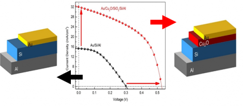
Cu2O is attractive for solar cells applications because it is abundant, nontoxic, and can be deposited at low temperatures and potentially at low cost. In this work, a passivated Si/cuprous oxide (Cu2O) hole-selective heterojunction with 0.53 V open-circuit voltage (VOC) is reported, a 37% increase over the state-of-the-art. The secret to achieving the record performance is in passivating the interface with a SiO2 layer that is so thin than carrier can quantum-mechanically “tunnel” through it. Such advances can further reduce the cost and solar photovoltaics.
References:
- P. Ravindra, R. Mukherjee and S. Avasthi, "Hole-Selective Electron-Blocking Copper Oxide Contact for Silicon Solar Cells," in IEEE Journal of Photovoltaics, vol. 7, no. 5, pp. 1278-1283, Sept. 2017.
doi: 10.1109/JPHOTOV.2017.2720619 - R. Mukherjee, P. Ravindra, S. Avasthi, “Ultra-Thin SiO2 Layers for Defect-Free Si/oxide Carrier Selective Contacts," 2017 MRS Spring Meeting, Phoenix, AZ, April 2017.
- P. Ravindra, R. Mukherjee, S. Avasthi, “Cu2O/Si Heterojunction Based Carrier Selective Contact for Silicon Photovoltaics," 2017 MRS Spring Meeting, Phoenix, AZ, April 2017.