A novel wafer scale technique for exact placement of two arrays of nanoparticles, with graphene as a spacer, has been developed. Placing two nanoparticles at such proximity gives rise to an extremely high field concentration in the gap between the two particles, which has enabled an extremely large near field enhancement, (E/EO) ~ 103. This has resulted in a huge photovoltage (in the order of A/W) and enhancement of the Raman signal (approx. 15 times) in single layer graphene [1].
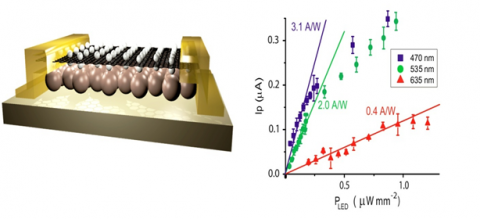
Figure: (Left) Schematic of the device for photocurrent measurement. (Right) Photoresponse of the device at 3 different wavelengths with respect to incident power.
[1] Debadrita Paria, Kallol Roy, Haobijam Johnson Singh, Shishir Kumar, Srinivasan Raghavan, Arindam Ghosh, and Ambarish Ghosh, Advanced Materials 27, 1751 (2015).