CeNSE operates a semi-production scale 3” GaN MOCVD reactor capable of growing high-quality epitaxial GaN films on Si, sapphire and SiC substrates. This system is primarily being used to develop nitride-based high power and high frequency HEMTs, UV sensors, and UV LEDs. In addition, the reactor supplies state-of-the-art GaN/AlGaN HEMTs to universities and strategic laboratories all over India, providing easy access to an otherwise very expensive and hard-to-procure strategic material.
1. High Power Switches
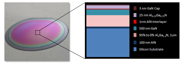
In collaboration with a team of seven professors from three different departments, CeNSE has been designing GaN power transistors for DC-DC conversion. The final goal of project is to develop a high electron-mobility transistor capable of switching 540 Amperes of current at 40 V in normally-on mode and to realize normally-off GaN HEMT which can carry 5 Ampere of current while blocking 600 V. The heart of the devices is the GaN HEMT stack, with world-class performance. Research is ongoing to reduce defects in the deposited GaN to minimize current leakage and heating, and to improve interface between GaN and AlGaN to reduce scattering.
GaN HEMT stack deposited on silicon wafer
Representative Publications
i) Xiaojun Weng, Srinivasan Raghavan, J. Acord, A. Jain, E. Dickey and J. M. Redwing, “Evolution of Threading Dislocations in MOCVD-Grown GaN films on Si,” Journal of Crystal Growth, 2007, 300, 217-222
ii) B. Sheldon, A. Bhandari, A. Bower, Srinivasan Raghavan and J. M. Redwing, “Steady State Tensile Stresses During Growth of Polycrystalline Films,” Acta. Materialia., 55, 4973, 2007.
iii) Jain, X. Weng, Srinivasan Raghavan, B. VanMil, T. Myers and J. Redwing, “Effect of polarity on the growth of InN thin films by MOCVD,” J. Appl. Phys., 104, 053112, 2008.
iv) Invited book chapter titled, “Group III-A Nitrides on Si: Stress and Microstructure” by Srinivasan Raghavan and Joan Redwing, in "III-V Compound Semiconductor: Integration with Silicon-based Microelectronics." Edited by Tingkai Li, Michael Mastro, Armin Dadgar, and Edwin L Piner, Dec, 2010, Pg. 209-257, CRC press.
2. Ultra-violet Optoelectronics
While red, green and now blue optoelectronic devices are ubiquitous. Ultra-violet LEDs, lasers and sensors are not that common. Ultra-violet rays are so energetic that they are not easy to manipulate in electronics devices. However UV optoelectronics has several applications. High-power UV LEDS can be used to make portable and efficient water purifiers, a desperate need in India. UV sensors can be used to study astronomical phenomenon, as well as remotely detect missile launches. The material system of choice for all these applications is alloys of GaN and AlN. Gallium Oxide, an emerging wide band gap material, is also gaining rapid traction among the device community in the world for high-performance UV detectors. CeNSE boasts of the some of the most sensitive UV detectors in the world, both in GaN and in Gallium Oxide* systems!
High-Power UV LED for Water Purification

UV Detector for Missile launch detection
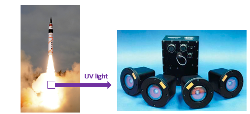
*In collaboration with Ohio State University, USA
Representative Publications
i) A. Singh Pratiyush, S. Krishnamoorthy, S. V. Solanke, Z. Xia, R. Muralidharan, S. Rajan, D. N. Nath, “High responsivity in molecular beam epitaxy grown β-Ga2O3 metal semiconductor metal solar blind deep UV photodetector”, Applied Physics Letters, 110, 221107 (2017)
ii) S. Rathkanthiwar, A. Kalra, S. V. Solanke, N. Mohtaa, R. Muralidharan, S. Raghavan, D. N. Nath, “Gain mechanism and carrier transport in high responsivity AlGaN-based solar blind metal semiconductor metal photodetectors”, Journal of Applied Physics, 121, 164502 (2017)
 Associate Professor |