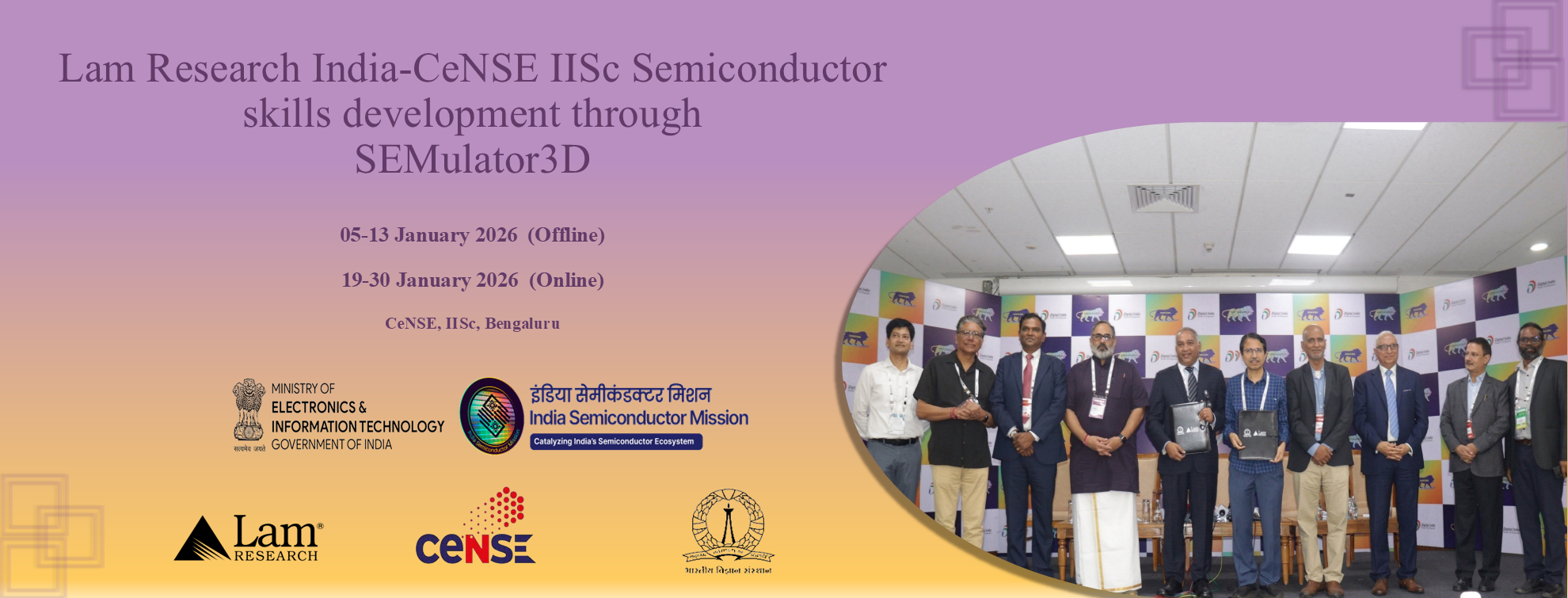
The program will create a cadre of 60000 engineers with employable skills for the semiconductor industry. The program will deliver training at scale using SEMulator3D®, an advanced EDA simulation platform from Lam Research. The program is being funded by the India Semiconductor Mission (ISM, https://ism.gov.in/) and the Ministry of Electronics and IT (MeitY, https://www.meity.gov.in/). Lam Research India is donating licenses. The program is being managed and executed by the Centre for Nanoscience and Engineering (CeNSE), Indian Institute of Science (IISc). This course is an unprecedented joint effort between industry and academia to create industry-relevant course content.
Offline Session - 01-09 June 2026
Centre for Nano Science and Engineering,Online Session - 22 June-07 July 2026
 Rangesh Raghavan
 Dinesh Munireddy
 Prof. Shankar Kumar Selvaraja
 Prof. Sushobhan Avasthi
SEMulator3D® is an industry-standard simulator that can impart training in semiconductor technology. The computing infrastructure needed is minimal and available at most institutes, so training can be rapidly scaled up. The training is suitable for students from diverse engineering backgrounds. While no simulator can replace hands-on experience, SEMulator3D® can take us 80% of the way. Internal industry training can manage the rest.
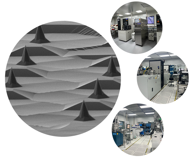
SEMulator3D® is a semiconductor process modeling platform that offers wide ranging technology development capabilities. Based on highly efficient physics-driven voxel modeling technology, SEMulator3D has a unique ability to model complete process flows. Starting from input design data, SEMulator3D follows an integrated process flow description to create the virtual equivalent of the complex, 3D structures created in the fab.SEMulator3D process modeling and analysis is used for fast and accurate “virtual fabrication” of advanced nano-fabrication processes, allowing engineers to understand manufacturing effects early in the development process and reduce time-consuming and costly silicon learning cycles.
Read more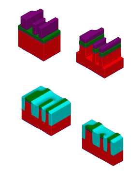 SEMulator3D can be used for process simulation and visulatization of the process flow
 Dr. Sushobhan Avasthi
  Dr. Shankar Kumar Selvaraja
 Nishant Kumar Sharma
Faculty from engineering schools so they can launch new courses on process technology in their respective institutes.
1-month session with two weeks of hands-on fabrication and characterisation training at CeNSE, IISc and two weeks of exposure to SEMUlator3D teaching material.
Hands-on Workshop will be conducted offline. SEMulator3D Demo & Lecture Sessions will be conducted online.
Yes, all the participants will receive a certificate of participation.
Yes, the outstation participants will be provided accommodation starting from one day before till the last day of the workshop subject to the availability of the funds.
Yes, TA will be provided as per GoI rules.


