
Research Breakthroughs
 |
Brightening the Future of DisplaysRead further: Nanoscale 2025, 17, 7753, https://pubs.rsc.org/en/content/articlelanding/2025/nr/d4nr05253f |
FRET-Driven Ultra-Vivid Pure-Red Emission Breakthrough in Polymer-Perovskite Hybrid Matrices
Integrating Perovskite nanocrystals (PeNCs) into polymer matrices unlocks an exciting pathway to dramatically enhance perovskite emission properties. By harnessing the power of Förster Resonance Energy Transfer (FRET) in polymer–PeNC composites, we achieve extraordinary improvements in photoluminescence efficiency, resulting in vibrant, ultra-pure red emission.
This breakthrough highlights the immense potential of polymer–PeNC blends to deliver highly efficient, vivid red-emitting materials, paving the way for next-generation displays and advanced optoelectronic applications.
 |
Breakthrough in Compensation free HEMT on Si for X Band Power PerformanceRead further: Phys. Status Solidi RRL, 2025, 2400409 at https://doi.org/10.1002/pssr.202400409 |
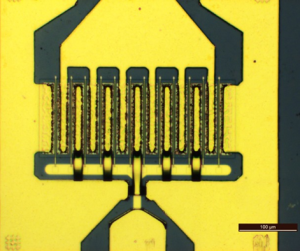
Successful demonstration of the microwave power performance of AlGaN/GaN HEMTs on silicon at X-band frequencies. Notably, this achievement was realized using a polarization-graded buffer without any compensation doping, such as iron or carbon, in the stack. At the 2 dB compression point, the devices delivered 8 W of output power at 10 GHz with a drain efficiency of 46%. Further improvements are anticipated with substrate thinning and enhanced thermal management.
 |
Tunable multi-color fiber laser source and applications in photoacoustic imagingRead this article published in Optics letters, Vol. 50., Issue. 7, pp 2223-2226 (2025) at https://doi.org/10.1364/OL.553618 |
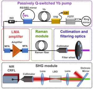
A novel tunable multi-color pulsed laser system as a compact, cost-effective alternative to supercontinuum and optical parametric oscillator (OPO) sources for biomedical imaging. Emitting in both the near-infrared (1060–1600 nm) and visible (530–600 nm) regions, it enables advanced applications like photoacoustic imaging (PAI). We demonstrate photoacoustic spectroscopy of lipids, a capability previously achievable only with OPOs, expanding the potential for biomedical research.
 |
Enhanced linewidth control in wavelength agile Raman fiber lasers using Fourier spectral shapingRead further: Optics Letters, Vol. 50, Issue 1, pp 201-204 (2025) at https://doi.org/10.1364/OL.544060 |
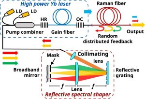
Cascaded Raman fiber lasers (CRFLs) can produce light at various wavelengths in the near-infrared (NIR) region, but their output is usually spectrally broad. In this work, researchers have introduced a new feedback method using Fourier spectral shaper that provides tunable filtered feedback, which helps narrow the output spectrum by about three times. This improvement is achieved without affecting the laser’s ability to tune across different wavelengths, while still delivering high power in the multi-watt range.
 |
Remote Characterization and Dissemination of Dispersion Compensated Ultrashort Pulses Through Dynamic Fiber Optic LinksRead further in IEEE, photonics journal at https://doi.org/10.1109/JPHOT.2025.3529627 |
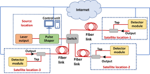
Ultrafast Lasers are complex pieces of equipment. It is desirable to have one source serve multiple locations and experiments for cost reduction. This can be accomplished through the dissemination of pulses to satellite locations through fiber optic links. However, the fidelity of pulses received and compensating dispersion effects requires thorough characterization. Requiring complex characterization equipment at all satellite location undoes the gains. In the work presented here, we overcome this problem.
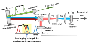 |
Remote characterization of nonlinear distortions in ultrashort pulses transmitted through dynamic fiber optic linksRead this article published in Optics Express, Vol. 33, Issue 2, pp. 2158-2168 at https://doi.org/10.1364/OE.545372 |
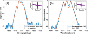
Here, we have introduced a method for remotely detecting the optical nonlinearities seen by ultrashort pulses in the fiber link. By integrating a custom-fabricated fixed delay interferometer with a quartz plate with partially reflecting Bragg mirrors to the detector module, we can accurately capture nonlinear distortions in sub-400 fs pulses. The detector module uses simple optics with non-movable parts and minimal footage, easily replicable at multiple target locations to facilitate pulse measurements. Thus, with robust delivery and characterization of both dispersive and nonlinear effects, this approach can significantly increase the efficacy of ultrafast laser sources and reduce overheads.
 |
Free Standing epitaxial oxides through remote epitaxyRead this article published in Nanoscale 17, 2025, pp. 2020-2031 at https://doi.org/10.1039/D4NR03356F |
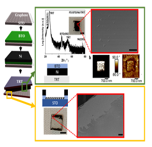
Epitaxial BaTiO3 (BTO) was grown via remote epitaxy using CVD graphene, and freestanding membranes were subsequently transferred onto Si. We identified a correlation between the graphene microstructure, its defect formation under pulsed laser deposition, and the crystalline quality of the deposited BTO film.
 |
High-Performance Graphene-Based Pressure SensorClick to read further: https://iopscience.iop.org/article/10.1088/1361-6439/ad5561 |
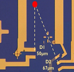
Researchers from the NEMS@CeNSE laboratory have created a highly sensitive graphene-based pressure sensor. It works by measuring changes in resonance frequency when pressure deforms a thin silicon diaphragm. This sensor is much more responsive than traditional silicon sensors, with a record-high performance of 20 kHz/kPa and potential up to 500 kHz/kPa. It can detect very small pressure changes (as low as 90 Pa). The design is simple, adaptable, and could be integrated into modern semiconductor manufacturing, making it highly practical. Read the complete article here at: More, S., & Naik, A. (2024). Graphene resonant pressure sensor with ultrahigh responsivity-range product. Journal of Micromechanics and Microengineering, 34(7), 075006.
 |
Enhanced Sensitivity in SERS Detection Using De-wetted Metal SubstratesClick to read further: https://doi.org/10.1016/j.apsusc.2024.161096 |
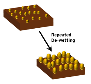
Surface-enhanced Raman spectroscopy (SERS) enhances molecular detection on metal surfaces or nanostructures. This study highlights that repeated de-wetting of metal thin films boosts SERS sensitivity over tenfold by creating closely spaced metal nanoclusters that amplify electromagnetic fields. The substrates detect Rhodamine 6G at sub-femtomolar levels and amino acids at micromolar levels. These findings suggest potential for integrating these substrates with nanopores for effective SERS-based sensing at confined, high-concentration conditions. Read the complete article here at: Pal, A., Roshini, R. A., & Varma, M. M. (2024). De-wetted gold nanostructures for SERS-based sensing of static and dynamic targets. Applied Surface Science, 678, 161096.
 |
Enhanced Analysis Method for Energy Loss in Piezoelectric MEMS DevicesClick to read further: https://ieeexplore.ieee.org/abstract/document/10705914 |
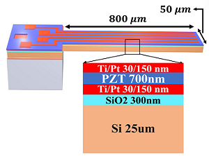
This research presents a new method using synchronized optical and electrical measurements to better analyze and improve piezo-MEMS devices. Piezoelectric microelectromechanical systems (MEMS) have great market potential due to their efficient energy conversion. However, energy loss in piezoelectric films can reduce device performance. Current methods to measure energy loss are not ideal for thin-film devices where energy storage and dissipation are spread across layers. The method is demonstrated using specialized MEMS components, enhancing accuracy and performance insights. Read the complete article here: Kumar, V., Tiwari, S., Pillai, G., Pratap, R., & Chandorkar, S. A. (2024). Synchronized Opto-Electro-Mechanical Measurements for Estimation of Energy Dissipation in Thin-Film-Piezoelectric-on-Substrate MEMS/NEMS Devices. Journal of Microelectromechanical Systems.
 |
Want to reduce the linewidth of Raman fiber lasers?Click to read further: https://opg.optica.org/oe/fulltext.cfm?uri=oe-32-12-20629&id=551029 |
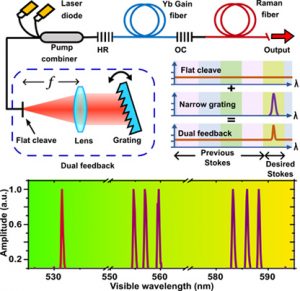
Use dual feedback! Then frequency double it to get >100 mW single mode power in visible.
Raman lasers can generate power at any wavelength, but the output spectrum is very broad. Researchers at CeNSE have found that by using the proposed “dual feedback” mechanism, linewidth reduction of ~ 5x is achieved at any wavelength. Frequency doubling this linewidth-reduced near infrared source, >100 mW single mode light of ~ 0.05 nm linewidth in green to yellow is generated.
This paper was published in Optics Express, Vol. 32, No.12, 3 June 2024.
 |
Waveguides for use in programmable photonic integrated circuits and neural network platformsClick to read further: https://pubs.aip.org/aip/apl/article-abstract/124/23/231105/3296495/Silicon-loaded-waveguide-in-sputter-deposited-PZT?redirectedFrom=fulltext |
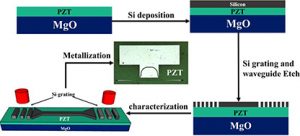
In this work, researchers developed an architecture that uses silicon-loaded PZT as the waveguide to realize a modulator to help overcome the electro-optic interaction issue faced in conventional architecture. The device enhanced EO response by 400% is attributed to the improved electro-optic overlap as well as PZT film quality.
The article was published in Applied physics Letters, AIP Publishing, 124, 231105, (2204).
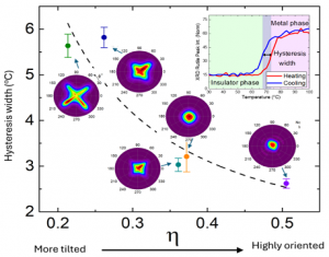 |
EPITAXIAL INTEGRATION OF VO2 ON TO SILICON UNVEILS TEXTURAL CONTROL OF HYSTERESISCheck out more details on this article at: https://www.sciencedirect.com/science/article/pii/S2589152924000826?via%3Dihub |
Vanadium Dioxide (VO₂) exhibits a fascinating metal-insulator transition (MIT) used in various applications. However, tailoring its phase transition hysteresis is crucial, for example sensors require minimal hysteresis while memories need a larger value.
In this study, researchers address two problems:
(a) epitaxial integration of VO2 onto Si(100), &
(b) use this as a model system to study the correlation between texture and phase-transition hysteresis in VO2 thin films.
The paper was published in Elsevier, Materialia, Vol. 34, May 2024, 102085.
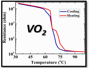 |
VO2 neuristors show large electro optic mechanical effectsCheck out more details on this article at: https://pubs.aip.org/aip/apr/article-abstract/11/2/021410/3283130/Large-electro-opto-mechanical-coupling-in-VO2?redirectedFrom=fulltext |
Researchers from CeNSE and SSCU, IISc demonstrated that VO2 based neuristors, produced electro-mechanical self-oscillatory behavior akin to biological neurons. High piezoelectric and electrooptic coefficients make it a promising candidate for diverse applications necessitating efficient energy conversion and optical modulation.
The research was published in AIP Publishing, Appl. Phys. Rev. 11, 021410 (2024).
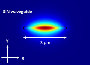 |
Shaping the Future: Embedded Si Gratings Enhance Thin Film SiN WaveguidesClick to read further: https://doi.org/10.1364/OE.488999 |
Researchers from the Photonics Research laboratory have developed an innovative silicon embedded grating coupler to improve fibre-chip coupling. The demonstration has far-reaching implications in quantum photonic integrated circuits, on-chip sensors, LiDAR and RADAR applications.
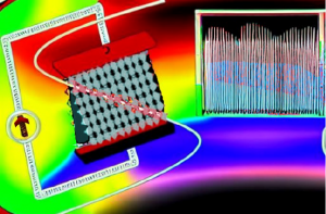 |
Unlocking Neuron-Like Self-Oscillations: Paving the Way for Low-Power Neuromorphic HardwareClick to read further: https://doi.org/10.1021/acsaelm.3c00549 |
The all-or-nothing law ensures the nerve cell fires at full strength or doesn’t. Members of the microsystems & fluctuations dissipation lab have demonstrated neuron like self-oscillations in thin films of NdNiO3.
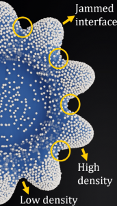 |
Mastering Impact Dynamics: How Particle-Coated Droplets Take Control of Pinch-Off PhenomenaClick further: https://doi.org/10.1016/j.jcis.2023.05.067 |
Research conducted by the Microfluidic Devices & Heterogeneous Systems lab has revealed critical insights into the factors that govern the stability of droplets during impact. This knowledge has significant implications for various applications, including printing, spraying, pesticide delivery, and cooling processes.
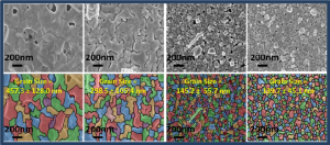 |
Breaking Barriers: Setting Record Mobility Values in Semiconductor InnovationClick to read more: https://doi.org/10.1039/D3TC00789H |
Researchers from the Heterojunction lab have systematically investigated the controlled growth of Cu2O using CVD and demonstrated record values of hole mobility and field-effect mobility. These CVD-deposited films are repeatable, scalable and relevant for transistors, displays drivers, and sensors.
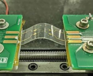 |
BEYOND PROTECTION: MOBILE SCREEN PROTECTORS AS SUBSTRATES FOR NEXT-GEN PIEZOTRONIC DEVICESClick to read more: https://ieeexplore.ieee.org/document/9998109 |
Piezotronics are the new-age semiconductor devices that find applications in sensors, flexible electronics and nanorobotics. Researchers at the NEMS@CeNSE lab have used these inexpensive, readily available, easily peelable flex screen protectors to fabricate 2D material devices.
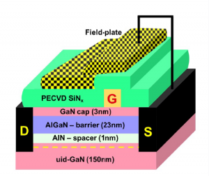 |
BOOSTING POWER AND EFFICIENCY: ENHANCING THE PERFORMANCE OF GAN HIGH ELECTRON MOBILITY TRANSISTORSClick to read more: https://ieeexplore.ieee.org/document/10049388 |
GaN HEMTs are crucial for high-power Radio Frequency (RF) applications like next-generation wireless communication and radars. Researchers from the Semiconductor Devices Lab have fabricated transistors on such a polarization-engineered platform displaying excellent dynamic performance, approaching state-of-the-art for GaN HEMTs on Silicon.
