Training on semiconductor
fabrication & characterization
![]()
![]()
Training on semiconductor
fabrication & characterization
Training on Semiconductor Fabrication & Characterization
Supported by Ministry of Tribal Affairs (MoTA)
![]()
08-19 June 2026
CeNSE, IISc, Bengaluru
Training on Semiconductor Fabrication & Characterization
Supported by Ministry of Tribal Affairs (MoTA)
![]()
08-19 June 2026
CeNSE, IISc, Bengaluru
Training on Semiconductor Fabrication & Characterization
Supported by Ministry of Tribal Affairs (MoTA)
![]()
08-19 June 2026
CeNSE, IISc, Bengaluru
Training on Semiconductor Fabrication & Characterization
Supported by Ministry of Tribal Affairs (MoTA)
![]()
08-19 June 2026
CeNSE, IISc, Bengaluru
Important Announcements
Aptitude test dates and details
Round 1
Application deadline – 4 April 2026
Aptitude test – 11 April 2026 (Saturday)
Round 2
Application deadline – 1 May 2026
Aptitude test – 9 May 2026 (Saturday)
Round 3
Application deadline – 30 May 2026
Aptitude test – 31 May 2026 (Saturday)
About
Preamble
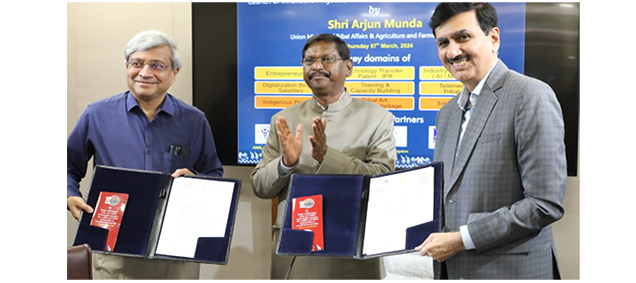
The Ministry of Tribal Affairs, in association with the Centre for Nano Science and Engineering at the Indian Institute of Science, has launched a unique program to upskill students from the tribal community in semiconductor technology. Semiconductor manufacturing is in resurgence due to the ₹77,000 Cr India Semiconductor Mission (ISM). ISM aims to establish multiple semiconductor fabs and packaging facilities in the country, which will require a skilled workforce with hands-on experience in semiconductor technology. The SemiCon talent committee projected a need of 30,000 by 2027 and 65000 by 2032. Tribal Communities can benefit by participating in this industry with well-paying jobs, provided they have the relevant skills. In this program IISc will build a dedicated training fab, so students with resource constraints can get state-of-art training at no cost. Faculty from tribal communities are also eligible to attend the training so they can increase their horizons with new courses and research.
Program OBJECTIVE
This program will train 450 students and faculty from the tribal community in semiconductor manufacturing technology.
The program is generously funded by the Ministry for Tribal Affairs (MoTA), Government of India, for the benefit of the tribal community. Students who pass the course will improve their knowledge and employability in the upcoming semiconductor manufacturing industry.
https://theprint.in/india/govt-to-train-tribal-students-in-semiconductor-technology-arjun-munda/1991922/
Program Format
- Training will be conducted in stages – foundation course and Advanced course. The Foundational course is a 60 hours program with online lectures and assignments. The advanced program is 90 hours with offline lectures, assignments and hands-on training in Bengaluru. Both courses are NSQF-certified, at levels 6.0 & 6.5, for foundational (https://nqr.gov.in/qualifications/3809) and advanced courses (https://nqr.gov.in/qualifications/3808), respectively.
- Selection is meritocratic. The selection to the foundational course is through an online test. The online test is based on content from a video lecture(s). The selection to the advanced courses will be from the graduating pool of foundational courses based on assignment performance.
- Minimum qualifications for students are: Pursuing (or rising) 4th year of UG Engineering OR pursuing (or rising) first year of M.Sc in the relevant field
- Faculty must be employed in a PG institute of higher learning for science or engineering.
Schedule for upcoming program
Online Foundation Training on Semiconductor Fabrication and Characterization
08-19 June, 2026 | 2 PM – 6 PM
Centre for Nano Science and Engineering
Indian Institute of Science, Bangalore
Organising Team
Mr. Somashekar P S (somashekarps@iisc.ac.in)
Ms. Sabiha Sultana (sabihas@iisc.ac.in)
Prof. Sushobhan Avasthi (savasthi@iisc.ac.in)
Team
|
Associate Professor |
Professor |
Associate Professor |
|
Professor |
COO - MNCF |
Schedule
Trainers

Aditya Sadhanala
Assistant Professor
Ambarish Ghosh
Professor

Dhavala Suri
Assistant Professor

Digbijoy N. Nath
Associate Professor
Pavan Nukala
Associate Professor
Sushobhan Avasthi
Associate Professor
Saurabh Chandorkar
Associate Professor
Sreetosh Goswami
Assistant Professor
Shankar Kumar Selvaraja
Associate Professor

Prosenjit Sen
Associate Professor
M. M. Nayak
Visiting Professor
ABOUT CeNSE
The Centre for Nano Science and Engineering (CeNSE) was established in 2010 to pursue interdisciplinary research on the nanoscale. Topics of interest include, but not limited to materials, electronics, MEMS/NEMS, photonics, biotechnology, and solar cells. If you have an exciting and revolutionary idea, come talk to us. We welcome both academic and industry collaborations.
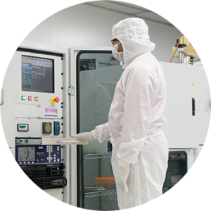
CeNSE houses a state-of-the art national nanofabrication centre (NNfC) with 14000 square feet of class 100/1000 clean room. It also houses a comprehensive micro nano characterization facility (MNCF) to conduct virtually any type of electrical, optical, mechanical and material characterization. Both of these are national user facilities are accessible to outside researchers for very reasonable charges.The Centre for Nano Science and Engineering (CeNSE) was established in 2010 to pursue interdisciplinary research on the nanoscale. Topics of interest include, but not limited to materials, electronics, MEMS/NEMS, photonics, biotechnology, and solar cells. If you have an exciting and revolutionary idea, come talk to us. We welcome both academic and industry collaborations.
CeNSE houses a state-of-the art national nanofabrication centre (NNfC) with 14000 square feet of class 100/1000 clean room. It also houses a comprehensive micro nano characterization facility (MNCF) to conduct virtually any type of electrical, optical, mechanical and material characterization. Both of these are national user facilities are accessible to outside researchers for very reasonable charges.
Cense Facilities
National Nanofabrication (NNfC)
National Nanofabrication Centre consisting of a comprehensive 14,000 sq. ft. clean-room facility with capability for:
Photolithography with resolution of 1 µm for optical and 10 nm for e-beam lithography.
Developing unit processes for chemical & physical vapour deposition (CVD) of most commonly used semiconductors and dielectrics, such as Si, SiGe, Ge, SiO2, SiNx, Al2O3, TiO2, etc.
Read more...
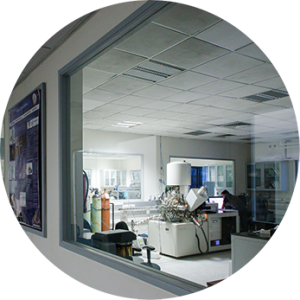
Micro and Nano Characterization Facility (MNCF)
The one of its kind micro and nano characterization facility (MNCF) aims to be a single shop for all a characterization needs of any nanofabrication process. It is rare to find such a comprehensive array of tools under a single roof, anywhere in the world.
Read more...
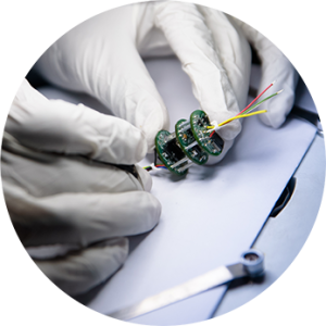
PACKAGING
IC Packaging facility has the complete capability to convert a wafer into a packaged device – from wafer sawing to wire bonding to precision welding. In addition, there are dedicated setups for pneumatic/hydraulic pressure calibration for pressure sensors and acoustic calibration for acoustic sensors.
Read more...
Events
2026-27 - Events Planned
| Sl No | Events | Dates | Venue | Days |
| 1 | Online Foundation Training on Semiconductor Fabrication and Characterization | 09-10 July 2026 | CeNSE, IISc, Bengaluru | 2 days |
| 2 | Advanced Training Program on Semiconductor Fabrication and Characterization | 13-21 July 2026 | CeNSE, IISc, Bengaluru | 9 days |
| 3 | Online Foundation Training on Semiconductor Fabrication and Characterization | 30-31 July 2026 | CeNSE, IISc, Bengaluru | 2 days |
| 4 | Advanced Training Program on Semiconductor Fabrication and Characterization | 03-11 August 2026 | CeNSE, IISc, Bengaluru | 9 days |
| 5 | Online Foundation Training on Semiconductor Fabrication and Characterization | 25 & 27 August 2026 | CeNSE, IISc, Bengaluru | 2 days |
| 6 | Advanced Training Program on Semiconductor Fabrication & Characterization | 31 August - 8 September 2026 | CeNSE, IISc, Bengaluru | 9 days |
| 7 | Online Foundation Training on Semiconductor Fabrication and Characterization | 17 & 18 September 2026 | CeNSE, IISc, Bengaluru | 2 days |
| 8 | Advanced Training Program on Semiconductor Fabrication & Characterization | 21 - 29 September 2026 | CeNSE, IISc, Bengaluru | 9 days |
| 9 | Online Foundation Training on Semiconductor Fabrication and Characterization | 8 & 9 October 2026 | CeNSE, IISc, Bengaluru | 2 days |
| 10 | Advanced Training Program on Semiconductor Fabrication & Characterization | 12-21 October 2026 | CeNSE, IISc, Bengaluru | 9 days |
| 11 | Online Foundation Training on Semiconductor Fabrication and Characterization | 29 & 30 October 2026 | CeNSE, IISc, Bengaluru | 2 days |
| 12 | Advanced Training Program on Semiconductor Fabrication & Characterization | 02-11 November 2026 | CeNSE, IISc, Bengaluru | 9 days |
2025-26 - Events Planned
| Sl No | Events | Dates | Venue | Days |
| 1 | Advanced Training Program on Semiconductor Fabrication and Characterization | 21-30 April 2025 | CeNSE, IISc, Bengaluru | 2 weeks |
| 2 | Online Foundation Training on Semiconductor Fabrication and Characterization | 02-13 June2025 | CeNSE, IISc, Bengaluru | 10 days |
| 3 | Advanced Training Program on Semiconductor Fabrication and Characterization | 21-30 July 2025 | CeNSE, IISc, Bengaluru | 2 weeks |
| 4 | Advanced Training Program on Semiconductor Fabrication and Characterization | 11-20 August 2025 | CeNSE, IISc, Bengaluru | 2 weeks |
| 5 | Advanced Training Program on Semiconductor Fabrication & Characterization | 25 August - 03 September 2025 | CeNSE, IISc, Bengaluru | 8 days |
| 6 | Advanced Training Program on Semiconductor Fabrication & Characterization | 08-16 September 2025 | CeNSE, IISc, Bengaluru | 7 days |
| 7 | Advanced Training Program on Semiconductor Fabrication & Characterization | 22-30 September 2025 | CeNSE, IISc, Bengaluru | 7 days |
| 8 | Advanced Training Program on Semiconductor Fabrication & Characterization | 06-14 October 2025 | CeNSE, IISc, Bengaluru | 7 days |
| 9 | Advanced Training Program on Semiconductor Fabrication & Characterization | 27 October - 4 November 2025 | CeNSE, IISc, Bengaluru | 7 days |
| 10 | Advanced Training Program on Semiconductor Fabrication & Characterization | 10-18 November 2025 | CeNSE, IISc, Bengaluru | 7 days |
| 11 | Advanced Training Program on Semiconductor Fabrication & Characterization | 24 November - 2 December 2025 | CeNSE, IISc, Bengaluru | 7 days |
| 12 | Online Foundation Training on Semiconductor Fabrication and Characterization | 08-19 December 2025 | CeNSE, IISc, Bengaluru | 10 days |
| 13 | Online Advanced Training on Semiconductor Fabrication and Characterization | 5th-6th February 2026 | CeNSE, IISc, Bengaluru | 2 days |
| 14 | Advanced Training Program on Semiconductor Fabrication & Characterization | 9th-17th February 2026 | CeNSE, IISc, Bengaluru | 9 days |
| 15 | Online Advanced Training on Semiconductor Fabrication and Characterization | 26th-27th February 2026 | CeNSE, IISc, Bengaluru | 2 days |
| 16 | Advanced Training Program on Semiconductor Fabrication & Characterization | 2nd-10th March 2026 | CeNSE, IISc, Bengaluru | 9 days |
| 17 | Online Advanced Training on Semiconductor Fabrication and Characterization | 26th-27th March 2026 | CeNSE, IISc, Bengaluru | 2 days |
| 18 | Advanced Training Program on Semiconductor Fabrication & Characterization | 30th March-8th April 2026 | CeNSE, IISc, Bengaluru | 10 days |
| 19 | Online Advanced Training on Semiconductor Fabrication and Characterization | 16th-17th April 2026 | CeNSE, IISc, Bengaluru | 2 days |
| 20 | Advanced Training Program on Semiconductor Fabrication & Characterization | 20th-28th April 2026 | CeNSE, IISc, Bengaluru | 9 days |
| 21 | Online Advanced Training on Semiconductor Fabrication and Characterization | 7th-8th May 2026 | CeNSE, IISc, Bengaluru | 2 days |
| 22 | Advanced Training Program on Semiconductor Fabrication & Characterization | 11th-19th May 2026 | CeNSE, IISc, Bengaluru | 9 days |
2024-25 - Events
| Sl No | Events | Dates | Venue | Days |
| 1 | Online Foundation Training on Semiconductor Fabrication and Characterization | 18-20 June 2024 | CeNSE, IISc, Bengaluru | 3 days |
| 2 | Advanced Training Program on Semiconductor Fabrication and Characterization | 19-28 August 2024 | CeNSE, IISc, Bengaluru | 2 weeks |
| 3 | Advanced Training Program on Semiconductor Fabrication and Characterization | 04-12 November 2024 | CeNSE, IISc, Bengaluru | 2 weeks |
| 4 | Online Foundation Training on Semiconductor Fabrication and Characterization | 09-20 December 2024 | CeNSE, IISc, Bengaluru | 2 weeks |
| 5 | Advanced Training Program on Semiconductor Fabrication and Characterization | 17-26 February 2025 | CeNSE, IISc, Bengaluru | 2 weeks |
| 6 | Advanced Training Program on Semiconductor Fabrication and Characterization | 10-19 March 2025 | CeNSE, IISc, Bengaluru | 2 weeks |
| 7 | Advanced Training Program on Semiconductor Fabrication and Characterization | 24 March - 02 April 2025 | CeNSE, IISc, Bengaluru | 2 weeks |
faqS
1. Who is eligible for registration?
Students from tribal community, pursuing (or rising) 4th year of UG Engineering (B.Tech / B.E.) OR pursuing (or rising) 2nd year of M.Sc in the relevant field.
2. Will the training program be online or offline?
Level 1 Program will be conducted online and Level 2 Program will be conducted offline.
3. Will I receive certificate of participation?
Yes, all the participants will receive a certificate of participation.
4. What is the procedure to apply for the Level 1 ( Online Foundation Training) Program ?
- Applicant should register click here
- After registration, if you meet the eligibility criteria, you will be sent a link for attending an online technical test for selection.
5. What is the procedure to apply for the Level 2 (Advanced Training) Program ?
Admission to the Level-2 (Advanced Training) Program is based on qualification criteria and not through direct application.
Participants must first successfully complete all Level-1 (Foundation) pre-requisites, which include:
Minimum required attendance in all live sessions
Timely submission of mandatory assignments
Completion of assessments/examination
Securing 70% or above in the final evaluation
Only candidates who meet all the above criteria will be shortlisted and formally invited to attend the 9-day Level-2 Advanced Training Program.
Eligible participants will receive an official communication with further instructions regarding confirmation of participation, schedule, and logistics.
6. Is it mandatory to attend Level 1(Foundation) Program in order to attend Level 2(Advanced) Program ?
It is mandatory.
7. Will the participants get accommodation while attending Level 2 Program ?
Yes, the outstation participants will be provided accommodation starting from one day before till the last day of the workshop subject to the availability of the funds.
8. Will the participants get Travel Allowance for attending Level 2 Program ?
Yes, subject to the availability of the funds, outstation participants will be provided Travel Allowance for train travel by 3-tier AC. No local TA (taxi or auto fare) will be reimbursed. If you are traveling by Air, you may claim partial reimbursement (up to 3-tier AC train fare only - as per rules).
Venue
Centre for Nano Science and Engineering
Indian Institute of Science,
Bengaluru - 560012. India.
Contact
Phone: 080-2293-4094