![]()
Training on semiconductor
fabrication & characterization
Foundational workshop on Semiconductor Manufacturing
![]()
09-17 April 2026
Foundational workshop on Semiconductor Manufacturing
![]()
09-17 April 2026
About
The Centre for Nano Science and Engineering (CeNSE) at the Indian Institute of Science (IISc) is excited to introduce a groundbreaking program to equip individuals with industry-relevant skills in semiconductor technology. This initiative is designed to address the growing demand for a skilled workforce in the rapidly expanding semiconductor industry.
As India emerges as a global hub for semiconductor manufacturing and packaging, driven by initiatives like the India Semiconductor Mission, the need for highly trained professionals has never been greater. Industry projections highlight a requirement of over 30,000 skilled personnel by 2027 and 65,000 by 2032. This program is designed to meet this demand by offering cutting-edge training and insights into semiconductor fabrication and characterization processes.
Delivered by renowned experts, the program offers:
- Comprehensive theoretical insights into semiconductor fabrication processes.
- Focus on contamination control, yield improvement, process variability, and metrology to ensure high-performance semiconductor fabrication.
- Exploration of MEMS, power electronics, advanced packaging, and cleanroom functionality, with insights into NNfC and MNCF facilities.
Whether you are an academic aiming to enhance your knowledge or an industry professional seeking to upskill, this program offers the perfect platform to stay ahead in the semiconductor revolution.
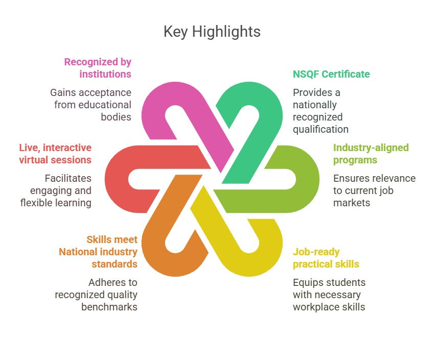
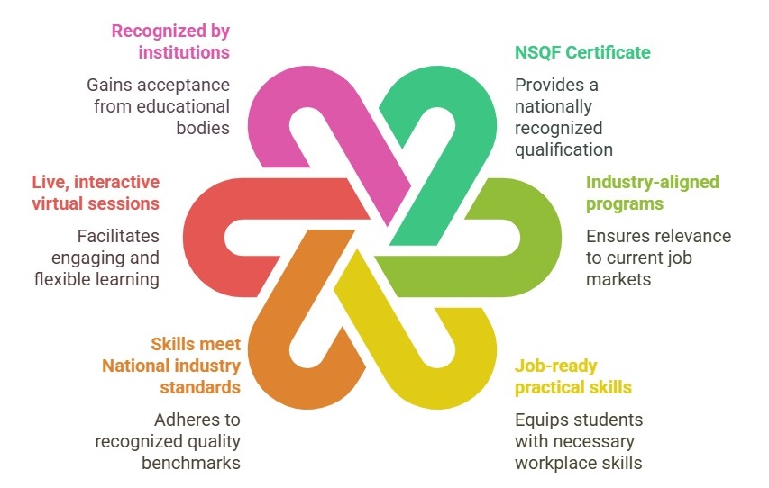
Key Highlights
Explore Course
Foundational workshop on Semiconductor Manufacturing
Course Description:
This course covers the fundamentals of nanofabrication, including unit processes, memory process flow, contamination control, and yield optimization. It explores process variability, metrology, and advanced topics like MEMS, power electronics, and semiconductor packaging. Participants will also gain insights into semiconductor equipment design, G S tapeout procedures, and cleanroom functionality, with an introduction to NNfC and MNCF facilities.
Duration : 60 Hours
Learning Outcomes:
- Gain a fundamental understanding of semiconductor manufacturing, the role of wafer fabs, and the essential equipment used in IC fabrication.
- Learn the principles of cleanroom design, including airflow, filtration, and utility integration, while understanding contamination control and safety protocols crucial for semiconductor production.
- Develop a clear understanding of the tape out flow, its critical steps, and the collaborative efforts required between design houses and foundries to ensure successful chip manufacturing.
- Understand process variability, yield engineering, and the importance of metrology in ensuring high-quality semiconductor production
- Learn how work is managed in world-class fabs, including economic considerations, engineering functions, and troubleshooting best practices for maintaining efficiency and quality control.
Who can apply:
- Professionals working in industries, startups, or related sectors with relevant expertise/interest in the field.
- Faculties and academicians with relevant expertise or interest in the field.
Last Date to Apply : 14th August 2025
Schedule for upcoming program
Online Foundation Training on Semiconductor Fabrication and Characterization
09-17 April, 2026 | 4 PM – 7 PM
Organizing Team
 Prof. Sushobhan Avasthi |
 Krishnan Shrinivasan |
 Seema Jaiswal |
 Sabiha Sultana |
 Somashekar P S |
 Akila Chetan |
 Pavani |
 Susan Sajna |
Schedule
Trainers

Sushobhan Avasthi

Saurabh Chandorkar
Shankar Kumar Selvaraja

Prosenjit Sen
Srinivasan Raghavan
Vijayaraghavan M
Ashutosh Bhabhe

Sandeep Koppikar
K L Narasimhan

Krishnan Shrinivasan
Javed G S

Gajendra M

Sabiha Sultana
ABOUT CeNSE
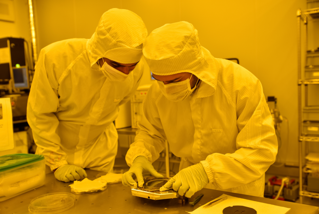
The Centre for Nano Science and Engineering (CeNSE) was established in 2010 to pursue interdisciplinary research on the nanoscale. Topics of interest include, but not limited to materials, electronics, MEMS/NEMS, photonics, biotechnology, and solar cells. If you have an exciting and revolutionary idea, come talk to us. We welcome both academic and industry collaborations.
CeNSE houses a state-of-the art national nanofabrication centre (NNfC) with 14000 square feet of class 100/1000 clean room. It also houses a comprehensive micro nano characterization facility (MNCF) to conduct virtually any type of electrical, optical, mechanical and material characterization. Both of these are national user facilities are accessible to outside researchers for very reasonable charges.The Centre for Nano Science and Engineering (CeNSE) was established in 2010 to pursue interdisciplinary research on the nanoscale. Topics of interest include, but not limited to materials, electronics, MEMS/NEMS, photonics, biotechnology, and solar cells. If you have an exciting and revolutionary idea, come talk to us. We welcome both academic and industry collaborations.
CeNSE houses a state-of-the art national nanofabrication centre (NNfC) with 14000 square feet of class 100/1000 clean room. It also houses a comprehensive micro nano characterization facility (MNCF) to conduct virtually any type of electrical, optical, mechanical and material characterization. Both of these are national user facilities are accessible to outside researchers for very reasonable charges.
Cense Facilities
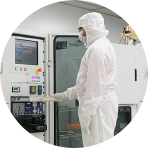
National Nanofabrication (NNfC)
National Nanofabrication Centre consisting of a comprehensive 14,000 sq. ft. clean-room facility with capability for:
Photolithography with resolution of 1 µm for optical and 10 nm for e-beam lithography.
Developing unit processes for chemical & physical vapour deposition (CVD) of most commonly used semiconductors and dielectrics, such as Si, SiGe, Ge, SiO2, SiNx, Al2O3, TiO2, etc.
Read more…
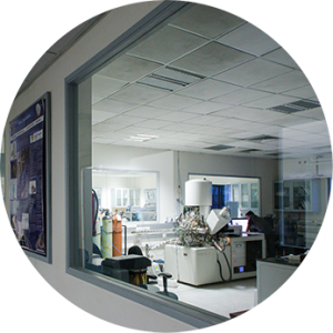
Micro and Nano Characterization Facility (MNCF)
The one of its kind micro and nano characterization facility (MNCF) aims to be a single shop for all a characterization needs of any nanofabrication process. It is rare to find such a comprehensive array of tools under a single roof, anywhere in the world.
Read more…
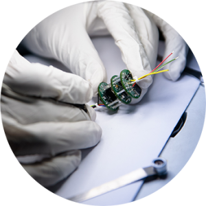
PACKAGING
IC Packaging facility has the complete capability to convert a wafer into a packaged device – from wafer sawing to wire bonding to precision welding. In addition, there are dedicated setups for pneumatic/hydraulic pressure calibration for pressure sensors and acoustic calibration for acoustic sensors.
Read more…
Events
2024-25 – Events Planned
| 1 | Online Foundation Training on Semiconductor Fabrication and Characterization | 07-15 April 2025 | 7 days |
| 2 | Online Foundation Training on Semiconductor Fabrication and Characterization | 18-26 August 2025 | 7 days |
Programme Fee
Fee Details
Academic : INR 5000+GST
Non-Academic/ Industries : INR 15000+GST
*For company collaborations , please reach us at workshop.cense@iisc.ac.in
faqS
1. Who is eligible for registration?
- Professionals working in industries, startups, or related sectors with relevant experience in the field.
- Faculties and academicians with relevant expertise or interest in the field.
2. Will the training program be online or offline?
The training will be conducted virtually in an online format.
3. Will I receive certificate of participation?
Yes, all attendees who complete the training sessions will receive a Participation Certificate.
4. Who is eligible for the NSQF certification?
This certification is only available to final-year students and above with an engineering background. Participants must also successfully complete all assessments to be eligible for this certification.
For any other queries [not listed here ]
Please write to workshop.cense@iisc.ac.in