Advanced Workshop on
Metrology & Nano-Characterization Techniques

Training on semiconductor
fabrication & characterization

About
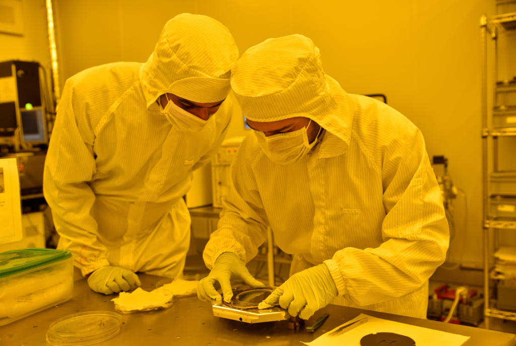
The Centre for Nano Science and Engineering (CeNSE) at the Indian Institute of Science (IISc) is organising an advanced workshop on metrology and nano-characterisation techniques, welcoming participants from academia, industry and start-ups. The programme is designed to develop practical, instrument-level proficiency in electrical, optical, structural and chemical characterisation methods that are fundamental to contemporary materials science, semiconductor processing and device development.
Delivered by CeNSE's expert scientific, and facility staff at the Micro and Nano Characterization Facility (MNCF), the programme integrates theory sessions with extensive practical laboratory experience utilising state-of-the-art instrumentation.
Over a four-day period, participants will have engaging learning with probe stations, electron microscopes, ion-beam systems and a broad range of spectroscopy and diffraction instruments, acquiring practical, instrument-level understanding that cannot be achieved through classroom instruction alone. Whether you are a researcher, an industrial engineer or a startup founder developing deep-tech hardware, this workshop provides a unique opportunity to train on national-facility characterisation infrastructure.
Key Highlights
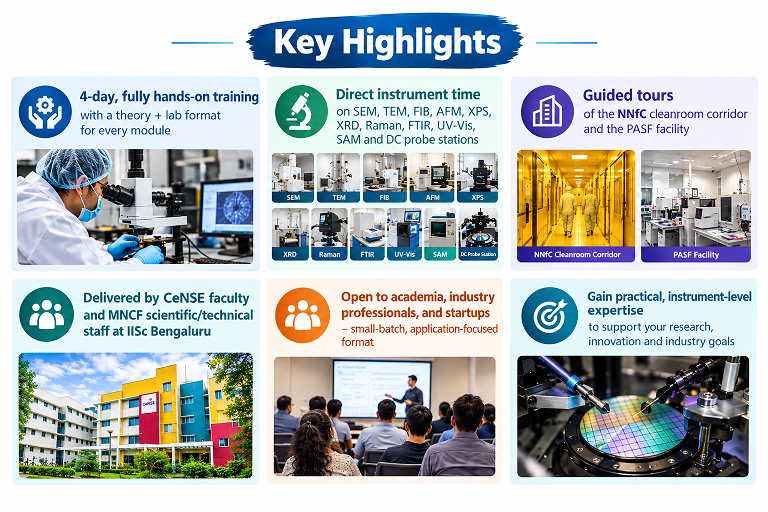
- 4-day, fully hands-on training with a theory + lab format for every module
- Direct instrument time on SEM, TEM, FIB, AFM, XPS, XRD, Raman, FTIR, UV-Vis, MSA and DC probe stations
- Training will be given by MNCF scientific/technical staff at IISc Bengaluru
- Open to academia, industry professionals, and startups — small-batch, application-focused format
Course Description
This training programme provides engineers with a practical understanding of the principal metrology and characterisation techniques employed in micro- and nanofabrication which can be applied in various branches of science and technology. Each module combines a theoretical lecture with a practical laboratory session, enabling participants to acquire both an understanding of the underlying physics and operational experience with the relevant instrumentation.
Duration: 4 days, approximately 8 contact hours per day.
Learning Outcomes:
-
Analyze and interpret electrical characterization data acquired through guided demonstrations on DC probe stations.
-
Evaluate surface morphologies and dynamic responses utilizing Atomic Force Microscopy (AFM) and Micro Systems Analyzer (MSA).
-
Interpret chemical, optical, and structural properties by exploring analytical workflows across XPS, XRD, Raman, FTIR, and UV-Visible spectroscopy platforms.
-
Comprehend advanced imaging workflows at the micro- and nano-scale via Scanning and Transmission Electron Microscopy (SEM/TEM).
-
Assess internal material and device architectures through site-specific milling and cross-sectioning demonstrations on Focused Ion Beam (FIB) systems.
Who should Attend:
- Faculty, postdocs, and research scholars from academic and R&D institutions
- Process, product, and device engineers from industry who are interested to develop understanding on characterization/metrology
- Founders and engineers from deep-tech / hardware startups needing hands-on exposure to advanced micro/nano characterization tools
Schedule for upcoming program
Organizing Team
 Dr. Suresha |
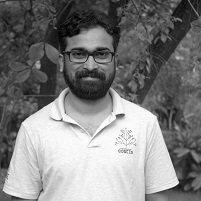 Dr. Nagabhushan |
 Seema Jaiswal |
 Pavani |
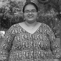 Susan Sajna |
 Akila Chetan |
ABOUT CeNSE
The Centre for Nano Science and Engineering (CeNSE) was established in 2010 at the Indian Institute of Science to pursue interdisciplinary research on the nanoscale, spanning materials, electronics, MEMS/NEMS, photonics, biotechnology, and solar cells.
CeNSE houses the National Nanofabrication Centre (NNfC), a state-of-the-art 14,000 sq. ft. Class 100/1000 cleanroom, and the Micro and Nano Characterization Facility (MNCF), which offers a comprehensive suite of electrical, optical, mechanical, and material characterization tools under a single roof. Both are national user facilities accessible to academic and industry researchers.
Cense Facilities
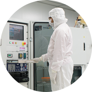
National Nanofabrication (NNfC)
National Nanofabrication Centre consisting of a comprehensive 14,000 sq. ft. clean-room facility with capability for:
Photolithography with resolution of 1 µm for optical and 10 nm for e-beam lithography.
Developing unit processes for chemical & physical vapour deposition (CVD) of most commonly used semiconductors and dielectrics, such as Si, SiGe, Ge, SiO2, SiNx, Al2O3, TiO2, etc.
Read more...
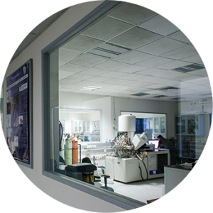
Micro and Nano Characterization Facility (MNCF)
The one of its kind micro and nano characterization facility (MNCF) aims to be a single shop for all a characterization needs of any nanofabrication process. It is rare to find such a comprehensive array of tools under a single roof, anywhere in the world.
Read more...
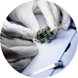
PACKAGING
IC Packaging facility has the complete capability to convert a wafer into a packaged device – from wafer sawing to wire bonding to precision welding. In addition, there are dedicated setups for pneumatic/hydraulic pressure calibration for pressure sensors and acoustic calibration for acoustic sensors.
Read more...
Programme Fee
Fee Details
- Academic Scholars, Students
- Faculty: Rs. 25,000 + GST
- Non-Academic and Industry: Rs. 50,000 + GST
- For AMAT : Rs. 40,000+GST
- For Accommodation: Rs. 10,000 + GST( Optional; applicable only for participants who opt for accommodation)
Upcoming Batches
• 25-29th October 2026
• 23-26th November 2026 (Deadline : 22nd November 2026 )
• 1-4th December 2026
(Registration will start soon)
faqS
1. Who is eligible to attend?
The workshop is open to all — faculty, students and research scholars from academic institutions, engineers and researchers from industry, and founders/engineers from startups working in materials, semiconductors, or deep-tech hardware.
2. Is the program hands-on?
Yes. Every module combines a theory lecture with an extensive lab session on the actual instrument, along with facility tours of NNfC and PASF.
3. Will lunch and tea breaks be provided?
Yes, tea breaks and lunch are scheduled daily as part of the program, as shown in the schedule above.
4. Will participants receive a certificate?
Yes, participants who complete the workshop will receive a Certificate of Participation from CeNSE, IISc.
5. Is there a registration fee?
Fees vary by participant category (academic / industry / startup). Please contact the organizing team for current fee details and registration.
Venue
Centre for Nano Science and Engineering (CeNSE), Indian Institute of Science, Bengaluru – 560012
Sessions are held across the Ground Floor Meeting Room (GF-01), Third Floor Meeting Room, Second Floor Conference Room (SF-01), and the MNCF laboratory.
For queries regarding this training program, please contact CeNSE, IISc Bengaluru.