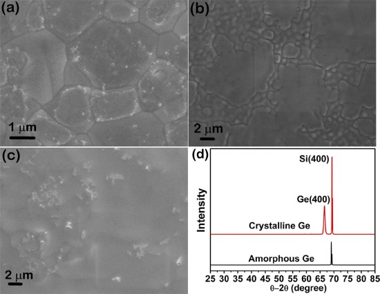
A wafer-scale method to obtain epitaxial germanium (Ge) on crystalline silicon (Si) using liquid-phase-crystallization (LPC) is presented. The technique provides a simple yet versatile method to grow epitaxial germanium on silicon with any crystallographic orientation: (100), (110) or (111). The process starts with amorphous Ge, which is melted and cooled in a controlled manner to form epitaxial germanium. LPC Ge films are continuous with an average grain-size of 2-5 μm. Rocking scan confirms that the LPC Ge is oriented with a threading dislocation density of <10$^9$ cm$^-2$. The phi-scan confirms that LPC germanium is epitaxial with Ge (100), Ge (110) and Ge (111) showing four-fold, two-fold, and three-fold symmetry, respectively. The epitaxial quality of the Ge is influenced by the cleanliness of the Ge/Si interface; rate of cooling and ambient gas during LPC; and Ge layer thickness. Best films are obtained for 1 μm thick LPC Ge(100), cooled at ~3-4 C/min in hydrogen ambient. Electron Hall mobility in these LPC Ge films is 736 cm$^2$/Vs, a high value that confirms the electronic quality of LPC Ge film.
Saloni Chaurasia, Nagaboopathy Mohan, Srinivasan Raghavan, Sushobhan Avasthi
AIP Advances,
2018
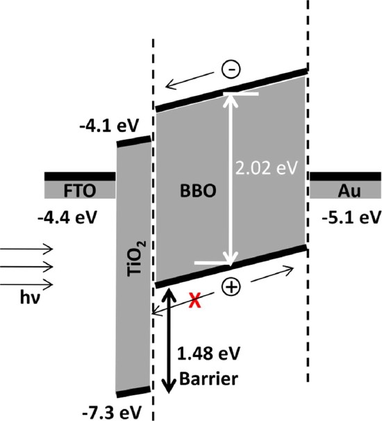
Metal-oxide/silicon carrier-selective heterojunctions 5 be a low-cost high-efficiency alternative to conventional silicon solar cells. Here, a passivated Si/cuprous oxide (Cu$_2$O) hole-selective heterojunction with high open-circuit voltage (VOC) is reported. Cu$_2$O is abundant, nontoxic, and can be deposited at low temperatures and potentially at low cost. The Si/Cu$_2$O heterojunction has a large conduction band offset of 0.9 eV and a negligible valence band offset, which blocks the transport of electrons but allows the transport of holes. The as-deposited hetero-interface is limited due to a high density of defects. However, the interface defect density can be reduced by a 1.2 nm thin tunneling SiO2 layer, which enables the realization of a Si/Cu$_2$O heterojunction solar cell with an open-circuit voltage (VOC) of 0.528 V, a 200 mV improvement over the state-of-the-art.
P. Ravindra, R. Mukherjee, S. Avasthi
IEEE Journal of Photovoltaics,
2017
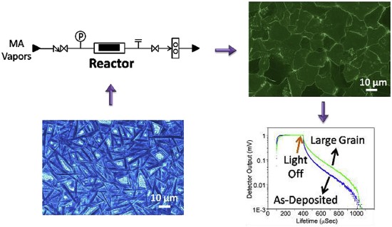
Spin coated perovskite thin films are known to have an issue of pinholes & poor morphology control which lead to poor device-to-device repeatability, that is an impediment to scale-up. In this work, Methylamine vapor annealing process is demonstrated which consistently leads to high-quality perovskite thin-films with an average grain-size of 10–15 μm. The improvement in film morphology enables improvement in effective carrier recombination lifetime, from 21 μs in as-deposited films to 54 μs in vapor-annealed films. The annealed films with large-grains are also more stable in ambient conditions. Devices made on annealed perovskite films are very consistent, with a standard deviation of only 0.7%. Methylamine vapor annealing process is a promising method of depositing large-grain CH$_3$NH$_3$PbI$_3$ films with high recombination lifetime and the devices with improved performance.
Arun Singh Chouhan, Naga Prathibha Jasti, Shreyash Hadke, Srinivasan Raghavan, Sushobhan Avasthi
Current Applied Physics,
2017
A hybrid approach to solar cells is demonstrated in which a silicon p–n junction, used in conventional silicon‐based photovoltaics, is replaced by a room‐temperature fabricated silicon/organic heterojunction. The unique advantage of silicon/organic heterojunction is that it exploits the cost advantage of organic semiconductors and the performance advantages of silicon to enable potentially low‐cost, efficient solar cells.
Sushobhan Avasthi, Stephanie Lee, Yueh-Lin Loo, James C. Sturm
Advanced Materials,
2011