![]()
Training on semiconductor
fabrication & characterization
Training on Semiconductor Fabrication & Characterization
Supported by Ministry of Tribal Affairs (MoTA)
![]()
2-13 June 2025
CeNSE, IISc, Bengaluru
Training on Semiconductor Fabrication & Characterization
Supported by Ministry of Tribal Affairs (MoTA)
![]()
2-13 June 2025
CeNSE, IISc, Bengaluru
Training on Semiconductor Fabrication & Characterization
Supported by Ministry of Tribal Affairs (MoTA)
![]()
2-13 June 2025
CeNSE, IISc, Bengaluru
Training on Semiconductor Fabrication & Characterization
Supported by Ministry of Tribal Affairs (MoTA)
![]()
2-13 June 2025
CeNSE, IISc, Bengaluru
Important Announcements
Round 1
Application deadline – 20th may 2025
Aptitude test – 24th & 25th May 2025
Round 2
Application deadline – 27th may 2025
Aptitude test – 31st May 2025
About
Preamble
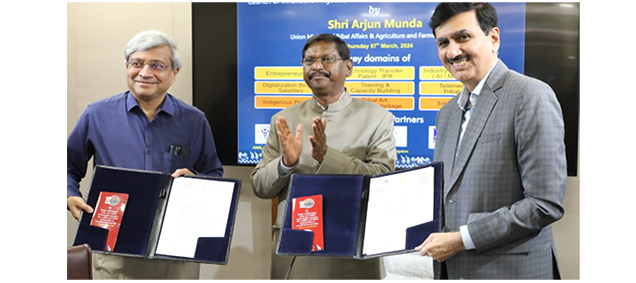
The Ministry of Tribal Affairs, in association with the Centre for Nano Science and Engineering at the Indian Institute of Science, has launched a unique program to upskill students from the tribal community in semiconductor technology. Semiconductor manufacturing is in resurgence due to the ₹77,000 Cr India Semiconductor Mission (ISM). ISM aims to establish multiple semiconductor fabs and packaging facilities in the country, which will require a skilled workforce with hands-on experience in semiconductor technology. The SemiCon talent committee projected a need of 30,000 by 2027 and 65000 by 2032. Tribal Communities can benefit by participating in this industry with well-paying jobs, provided they have the relevant skills. In this program IISc will build a dedicated training fab, so students with resource constraints can get state-of-art training at no cost. Faculty from tribal communities are also eligible to attend the training so they can increase their horizons with new courses and research.
Program OBJECTIVE
This program will train 450 students and faculty from the tribal community in semiconductor manufacturing technology.
The program is generously funded by the Ministry for Tribal Affairs (MoTA), Government of India, for the benefit of the tribal community. Students who pass the course will improve their knowledge and employability in the upcoming semiconductor manufacturing industry.
https://theprint.in/india/govt-to-train-tribal-students-in-semiconductor-technology-arjun-munda/1991922/
Program Format
- Training will be conducted in stages – foundation course and Advanced course. The Foundational course is a 60 hours program with online lectures and assignments. The advanced program is 90 hours with offline lectures, assignments and hands-on training in Bengaluru. Both courses are NSQF-certified, at levels 6.0 & 6.5, for foundational (https://nqr.gov.in/qualifications/3809) and advanced courses (https://nqr.gov.in/qualifications/3808), respectively.
- Selection is meritocratic. The selection to the foundational course is through an online test. The online test is based on content from a video lecture(s). The selection to the advanced courses will be from the graduating pool of foundational courses based on assignment performance.
- Minimum qualifications for students are: Pursuing (or rising) 4th year of UG Engineering OR pursuing (or rising) first year of M.Sc in the relevant field
- Faculty must be employed in a PG institute of higher learning for science or engineering.
Schedule for upcoming program
Online Foundation Training on Semiconductor Fabrication and Characterization
02-13 June, 2025 | 2 PM – 6 PM
Centre for Nano Science and Engineering
Indian Institute of Science, Bangalore
Organising Team
Mr. Somashekar P S (somashekarps@iisc.ac.in)
Ms. Sabiha Sultana (sabihas@iisc.ac.in)
Prof. Sushobhan Avasthi (savasthi@iisc.ac.in)
Team
 Prof. Sushobhan Avasthi |
 Prof. Srinivasan Raghavan |
 Prof. Shankar Kumar Selvaraja |
 Prof. Akshay Naik |
 Dr. Suresha S J |
Schedule
Program schedule will be
updated soon…
Trainers
Dr. Aditya Sadhanala
Dr. Ambarish Ghosh
Dr. Dhavala Suri
Dr. Digbijoy N. Nath
Dr. Pavan Nukala
Dr. Sushobhan Avasthi
Dr. Saurabh Chandorkar
Dr. Sreetosh Goswami
Dr. Shankar Kumar Selvaraja
Dr. Prosenjit Sen
Dr. M. M. Nayak
ABOUT CeNSE
The Centre for Nano Science and Engineering (CeNSE) was established in 2010 to pursue interdisciplinary research on the nanoscale. Topics of interest include, but not limited to materials, electronics, MEMS/NEMS, photonics, biotechnology, and solar cells. If you have an exciting and revolutionary idea, come talk to us. We welcome both academic and industry collaborations.
CeNSE houses a state-of-the art national nanofabrication centre (NNfC) with 14000 square feet of class 100/1000 clean room. It also houses a comprehensive micro nano characterization facility (MNCF) to conduct virtually any type of electrical, optical, mechanical and material characterization. Both of these are national user facilities are accessible to outside researchers for very reasonable charges.The Centre for Nano Science and Engineering (CeNSE) was established in 2010 to pursue interdisciplinary research on the nanoscale. Topics of interest include, but not limited to materials, electronics, MEMS/NEMS, photonics, biotechnology, and solar cells. If you have an exciting and revolutionary idea, come talk to us. We welcome both academic and industry collaborations.
CeNSE houses a state-of-the art national nanofabrication centre (NNfC) with 14000 square feet of class 100/1000 clean room. It also houses a comprehensive micro nano characterization facility (MNCF) to conduct virtually any type of electrical, optical, mechanical and material characterization. Both of these are national user facilities are accessible to outside researchers for very reasonable charges.
Cense Facilities
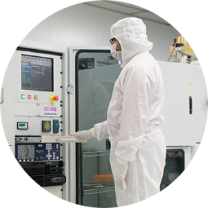
National Nanofabrication (NNfC)
National Nanofabrication Centre consisting of a comprehensive 14,000 sq. ft. clean-room facility with capability for:
Photolithography with resolution of 1 µm for optical and 10 nm for e-beam lithography.
Developing unit processes for chemical & physical vapour deposition (CVD) of most commonly used semiconductors and dielectrics, such as Si, SiGe, Ge, SiO2, SiNx, Al2O3, TiO2, etc.
Read more…
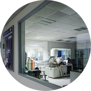
Micro and Nano Characterization Facility (MNCF)
The one of its kind micro and nano characterization facility (MNCF) aims to be a single shop for all a characterization needs of any nanofabrication process. It is rare to find such a comprehensive array of tools under a single roof, anywhere in the world.
Read more…
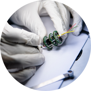
PACKAGING
IC Packaging facility has the complete capability to convert a wafer into a packaged device – from wafer sawing to wire bonding to precision welding. In addition, there are dedicated setups for pneumatic/hydraulic pressure calibration for pressure sensors and acoustic calibration for acoustic sensors.
Read more…
Events
2025-26 – Events Planned
| Sl No | Events | Dates | Venue | Days |
| 1 | Advanced Training Program on Semiconductor Fabrication and Characterization | 21-30 April 2025 | CeNSE, IISc, Bengaluru | 2 weeks |
| 2 | Online Foundation Training on Semiconductor Fabrication and Characterization | 02-13 June2025 | CeNSE, IISc, Bengaluru | 10 days |
| 3 | Advanced Training Program on Semiconductor Fabrication and Characterization | 21-30 July 2025 | CeNSE, IISc, Bengaluru | 2 weeks |
| 4 | Advanced Training Program on Semiconductor Fabrication and Characterization | 11-20 August 2025 | CeNSE, IISc, Bengaluru | 2 weeks |
| 5 | Advanced Training Program on Semiconductor Fabrication and Characterization | 08-17 September 2025 | CeNSE, IISc, Bengaluru | 2 weeks |
| 6 | Advanced Training Program on Semiconductor Fabrication and Characterization | 06-15 October 2025 | CeNSE, IISc, Bengaluru | 2 weeks |
| 7 | Online Foundation Training on Semiconductor Fabrication and Characterization | 08-19 December 2025 | CeNSE, IISc, Bengaluru | 10 days |
| 8 | Advanced Training Program on Semiconductor Fabrication and Characterization | January 2026 | CeNSE, IISc, Bengaluru | 2 weeks |
2024-25 – Events
| Sl No | Events | Dates | Venue | Days |
| 1 | Online Foundation Training on Semiconductor Fabrication and Characterization | 18-20 June 2024 | CeNSE, IISc, Bengaluru | 3 days |
| 2 | Advanced Training Program on Semiconductor Fabrication and Characterization | 19-28 August 2024 | CeNSE, IISc, Bengaluru | 2 weeks |
| 3 | Advanced Training Program on Semiconductor Fabrication and Characterization | 04-12 November 2024 | CeNSE, IISc, Bengaluru | 2 weeks |
| 4 | Online Foundation Training on Semiconductor Fabrication and Characterization | 09-20 December 2024 | CeNSE, IISc, Bengaluru | 2 weeks |
| 5 | Advanced Training Program on Semiconductor Fabrication and Characterization | 17-26 February 2025 | CeNSE, IISc, Bengaluru | 2 weeks |
| 6 | Advanced Training Program on Semiconductor Fabrication and Characterization | 10-19 March 2025 | CeNSE, IISc, Bengaluru | 2 weeks |
| 7 | Advanced Training Program on Semiconductor Fabrication and Characterization | 24 March – 02 April 2025 | CeNSE, IISc, Bengaluru | 2 weeks |
faqS
1. The Centre for Nano Science and Engineering (CeNSE) was established in 2010 to pursue interdisciplinary research on the nanoscale?
Your content goes here. Edit or remove this text inline or in the module Content settings. You can also style every aspect of this content in the module Design settings and even apply custom CSS to this text in the module Advanced settings.
2. The Centre for Nano Science and Engineering (CeNSE) was established in 2010 to pursue interdisciplinary research on the nanoscale?
Your content goes here. Edit or remove this text inline or in the module Content settings. You can also style every aspect of this content in the module Design settings and even apply custom CSS to this text in the module Advanced settings.
3. The Centre for Nano Science and Engineering (CeNSE) was established in 2010 to pursue interdisciplinary research on the nanoscale?
Your content goes here. Edit or remove this text inline or in the module Content settings. You can also style every aspect of this content in the module Design settings and even apply custom CSS to this text in the module Advanced settings.
4. The Centre for Nano Science and Engineering (CeNSE) was established in 2010 to pursue interdisciplinary research on the nanoscale?
Your content goes here. Edit or remove this text inline or in the module Content settings. You can also style every aspect of this content in the module Design settings and even apply custom CSS to this text in the module Advanced settings.
5. The Centre for Nano Science and Engineering (CeNSE) was established in 2010 to pursue interdisciplinary research on the nanoscale?
Your content goes here. Edit or remove this text inline or in the module Content settings. You can also style every aspect of this content in the module Design settings and even apply custom CSS to this text in the module Advanced settings.
6. The Centre for Nano Science and Engineering (CeNSE) was established in 2010 to pursue interdisciplinary research on the nanoscale?
Your content goes here. Edit or remove this text inline or in the module Content settings. You can also style every aspect of this content in the module Design settings and even apply custom CSS to this text in the module Advanced settings.
7. The Centre for Nano Science and Engineering (CeNSE) was established in 2010 to pursue interdisciplinary research on the nanoscale?
Your content goes here. Edit or remove this text inline or in the module Content settings. You can also style every aspect of this content in the module Design settings and even apply custom CSS to this text in the module Advanced settings.
8. The Centre for Nano Science and Engineering (CeNSE) was established in 2010 to pursue interdisciplinary research on the nanoscale?
Your content goes here. Edit or remove this text inline or in the module Content settings. You can also style every aspect of this content in the module Design settings and even apply custom CSS to this text in the module Advanced settings.