Welcome to the Functional Thin Films and Electron Microscopy Laboratory at CeNSE, IISc Bangalore. We are an experimental group, who routinely challenge the conventional wisdom of materials design for electronic, MEMS, electro-optic and neuromorphic applications. Our answer more often than not is defect-engineering. We work on a wide variety of materials systems spanning from complex oxides to simple oxides to chalcogenides.
Here is a glimpse of our research activity:
Unconventional Ferroelectrics
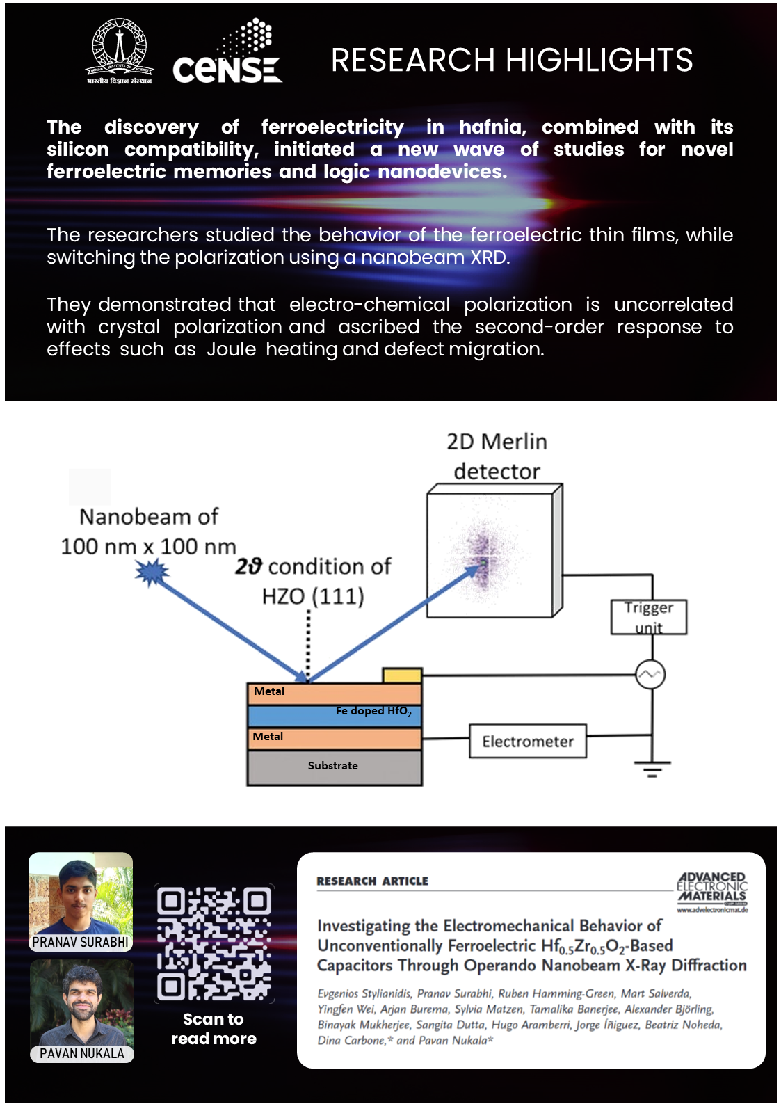
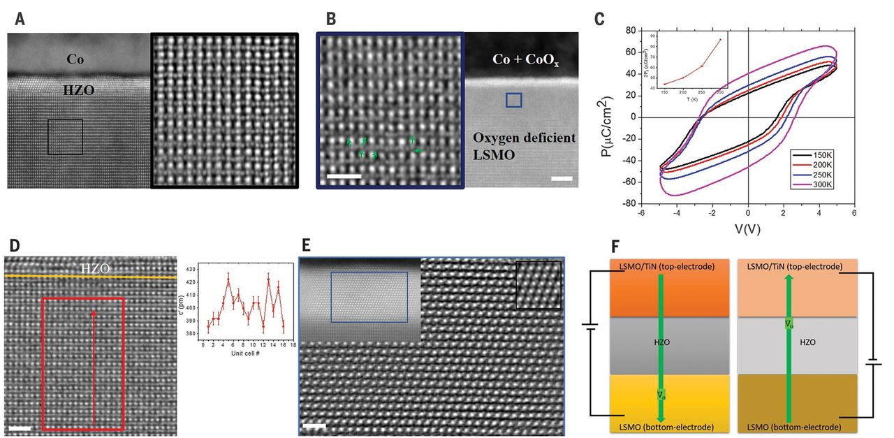
In-situ electron microscopy, structure-property correlation study: Oxygen vacancy migration in hafnia-based ferroelectrics is very much intertwined with its ferroelectric switching. More details here.