![]()
Training on semiconductor
fabrication & characterization
Winter School 2025
A conference to shape the future of semiconductor technology
![]()
08-19 December 2025
Winter School 2025
A conference to shape the future of semiconductor technology
![]()
08-19 December 2025
About
CeNSE, IISc is launching a Winter School in semiconductor technology that is targeted at UG/PG students intrigued by semiconductor manufacturing. Semiconductor manufacturing is having a moment. For the first time, India is making significant investments in manufacturing advanced semiconductor devices. The Government of India has launched the ₹77000 Cr Indian Semiconductor Mission (ISM), under which commercial semiconductor foundries are being built in the country for the first time.
The upcoming facilities require a highly skilled workforce, estimated by MeitY’s talent committee to be 30,000 by 2027 and 65,000 by 2032. The Winter School is our attempt to deliver training in semiconductor technology at scale. ISM can only succeed if promising youngsters participate in it.
The training program will be of 2 weeks duration. The fees for enrolling to this Winter School is Rs. 1180/-.
Schedule for upcoming program
Winter School 2025
08-19 December, 2025
Organizing Team
 Prof. Sushobhan Avasthi |
 Sabiha Sultana |
 Seema Jaiswal |
 Somashekar P S |
 Susan Sajna |
 Pavani KV |
 Akila Chetan |
Schedule
ABOUT CeNSE
The Centre for Nano Science and Engineering (CeNSE) was established in 2010 to pursue interdisciplinary research on the nanoscale. Topics of interest include, but not limited to materials, electronics, MEMS/NEMS, photonics, biotechnology, and solar cells. If you have an exciting and revolutionary idea, come talk to us. We welcome both academic and industry collaborations.
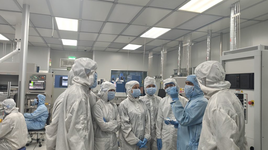
CeNSE houses a state-of-the art national nanofabrication centre (NNfC) with 14000 square feet of class 100/1000 clean room. It also houses a comprehensive micro nano characterization facility (MNCF) to conduct virtually any type of electrical, optical, mechanical and material characterization. Both of these are national user facilities are accessible to outside researchers for very reasonable charges.The Centre for Nano Science and Engineering (CeNSE) was established in 2010 to pursue interdisciplinary research on the nanoscale. Topics of interest include, but not limited to materials, electronics, MEMS/NEMS, photonics, biotechnology, and solar cells. If you have an exciting and revolutionary idea, come talk to us. We welcome both academic and industry collaborations.
CeNSE houses a state-of-the art national nanofabrication centre (NNfC) with 14000 square feet of class 100/1000 clean room. It also houses a comprehensive micro nano characterization facility (MNCF) to conduct virtually any type of electrical, optical, mechanical and material characterization. Both of these are national user facilities are accessible to outside researchers for very reasonable charges.
Cense Facilities

National Nanofabrication (NNfC)
National Nanofabrication Centre consisting of a comprehensive 14,000 sq. ft. clean-room facility with capability for:
Photolithography with resolution of 1 µm for optical and 10 nm for e-beam lithography.
Developing unit processes for chemical & physical vapour deposition (CVD) of most commonly used semiconductors and dielectrics, such as Si, SiGe, Ge, SiO2, SiNx, Al2O3, TiO2, etc.
Read more…
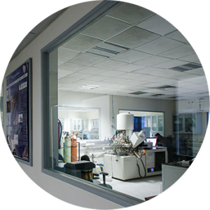
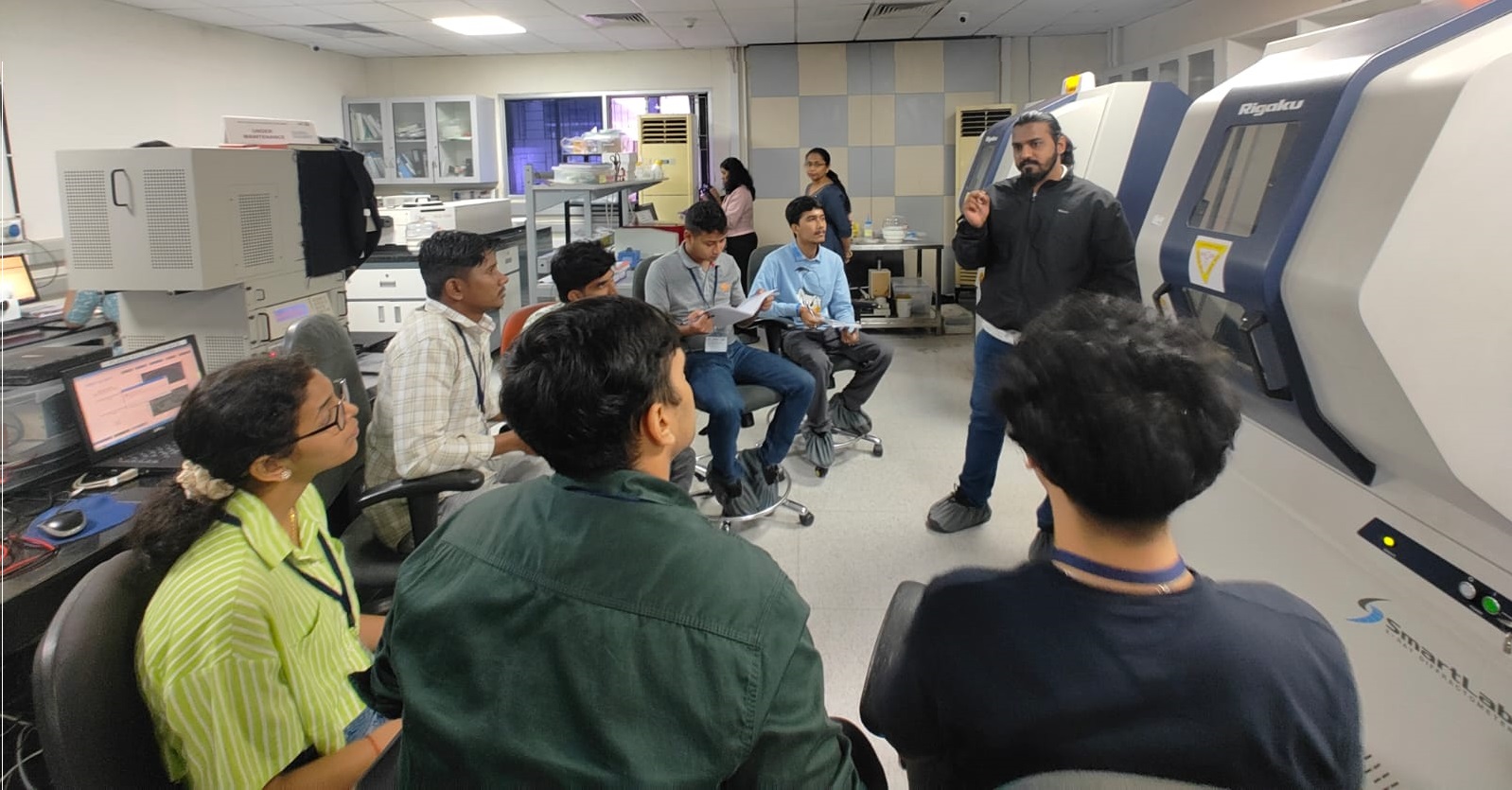
Micro and Nano Characterization Facility (MNCF)
The one of its kind micro and nano characterization facility (MNCF) aims to be a single shop for all a characterization needs of any nanofabrication process. It is rare to find such a comprehensive array of tools under a single roof, anywhere in the world.
Read more…
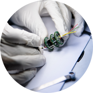
Packaging and Systems Facility (PASF)
Packaging & Systems Facility ( PASF) Packaging and Systems Facility with an area of 2500 SFT is an ESD safe workspace which houses various electronic test & measurement equipments. The PASF offers Hardware and Embedded Design Services to its Users and in addition ESD work stations, soldering and desoldering stations, electronic modules & components and processors’ based evaluation kits.
Read more…
faqS
1. Who is eligible for registration?
- UG/PG students are eligible to register for the program.
2. Will the winter school will be online or offline ?
Winter school will be conducted online.
3. How much is the registration fee?
- Academic Scholars or Students: Rs.1,000+GST
-
Academic Faculty or Staff: Rs.10,000+GST
-
Industry or Startup: Rs.30,000+GST
4. Will I receive certificate of participation?
Yes, Upon successful completion of the program, participants will be eligible for a certificate of participation issued by CeNSE, provided they meet the performance and attendance requirements.
5. Can I cancel my registration after fee payment and will I get a refund?
Registration fees is non-refundable.
It should be noted that fees once paid during registration will not be refunded under any circumstances. Please fill the registration form only if you will be attending the winter school for sure.
6. What is the procedure to apply for the Winter School Program ?
Applicant should register
For any other queries [not listed here ]
Please write to workshop.cense@iisc.ac.in
Contact
Phone: +91 080-2293-4094