Facilities
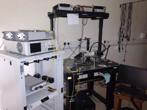
Optical Characterisation
Optical and electro-optic characterisation facility has seen steady growth since 2015. We are currently building chracterization facility for the photonic integrated circuit that will enable optical/electro-optic characterisation of circuits in telecom wavelength band.
Photonics EDA Infrastructure
For optical design and simulation, we house a combination of proprietary and open-source computation tools. For modest simulation, the group has powerful workstations, and for heavy loads, we use supercomputer infrastructure available in Supercomputer Education and Research Centre (SERC).
Device and Circuit Fabrication
Photonic devices and circuits are fabricated at National Nano Fabrication Centre (NNfC) located in Centre for Nano Science and Engineering (CeNSE). The facility houses complete fabrication tool-set required for fabricating photonic integrated circuits. Research students and staff are trained to independently use tools required for their research. More details can be found at NNfC website.
Electrical Characterisation
Electrical characterization of the device that we fabricate is done at Micro and Nano Characterization Facility (MNCF) located in Centre for Nano Science and Engineering (CeNSE). MNCF has a comprehensive set of characterization tool for not only electrical but also material and mechanical characterization tool. More details can be found at MNCF website.