
Prof. Rudra Pratap's Research Group
Liquid Metal Electromigration
Electromigration is a unidirectional mass transport phenomenon controlled by diffusion and driven by an applied electric field. The recent discovery of the phenomenon in liquid materials has generated a new field of study with various and promising applications, specifically to modern fabrication techniques.
Liquid metal electromigration can be observed simply by placing a metal bead on a conducting film path. As the metal bead melts, it starts to flow in a certain direction determined by Joule heating and the electromigration force induced by an applied electric field across the conducting film. In other experiments, we have observed the symmetric flow of an intermediate liquid compound which forms around a cathode point when probed on a Cr-film at a certain applied potential across the anode and cathode.
Electromigration, in general, is a damaging phenomenon with a strong dependence on ambient conditions. In our research we have been testing different ambient conditions to see their effect on the electromigration-induced damages to Cr-film. With repeated observations and measurements, we have successfully been able to boost or prevent the electromigration effect by changing ambient parameters.
Ultimately, our goal is to be able to precisely predict the pattern generated on the thin film by gaining a fundamental understanding of the mechanism and the various control parameters. Precise control over the phenomena is expected to accelerate the recently developed Electrolithography technique for device fabrication.
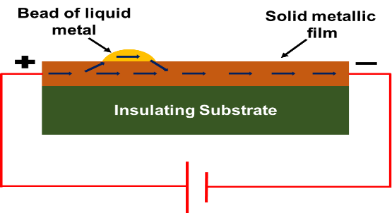
Schematic diagram of a metal bead placed on a conducting film to observe the electromigration effect.
Lithography by Exploiting Electromigration
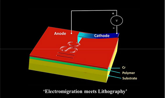
Electrolithography is a new patterning technique based on electric-field induced material transport. Electrolithography can be used for drawing patterns having dimensions from a few nanometres to a few hundred micrometres. It does not require any e-beam or UV source and it can be carried out under ambient conditions.
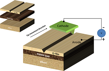
Electric current, assisted by Joule heating, can induce the long-range flow of material; this phenomenon is known as liquid electromigration. In the particular case of a thin Cr film deposited on an insulating substrate, the application of a high electric-field between two point electrodes results in liquefaction and subsequent flow of the liquefied material in a radially symmetric fashion away from the cathode. In electrolithography, we use a thin Cr film as a masking layer and use a polymer layer beneath it as a pattern transfer layer. A negatively biased scanning probe is used to perform electromigration on the metal film to generate patterns.
Using this technique, the best resolutions achieved are of 9 nm on the polymer and of 40 nm when transferring the pattern to another material. In common SPL techniques, the depth of the patterns drawn on the polymer layer are often extremely small. Thus, transferring those patterns to other materials becomes difficult. However, in electrolithography processes, the etch depth in the polymer is same as the polymer layer thickness (usually ~ 200 nm). Therefore, patterns are easily transferrable and the final patterned structures can be as thick as 100 nm, allowing them to be used in microelectronic devices. In electrolithography, the polymer is used only to transfer the patterns. Therefore, any polymer and corresponding developer can be used which removes the need for the costly and toxic chemicals normally used in lithography processes. We have also demonstrated the technique of direct writing on Cr film, deposited on a glass substrate, used to make lithography masks.
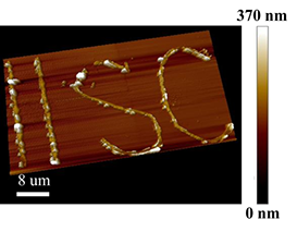
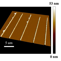
Patterns Generated by Electrolithography
MEMS Lab, Centre for Nano Science and Engineering, Indian Institute of Science. Bangalore-560012
Phone: +91 (80) 2293 3250, +91 (80) 2360 8659 Fax: +91 (80) 2360 1648 Email: pratap@iisc.ac.in, memslab@iisc.ac.in