
Prof. Rudra Pratap's Research Group
Our interest in different piezoMEMS devices led our attention to material development for sensor fabricaion. Material development for sensors is unique in a way that it requires a certain material stack to be follower. For example any piezoMEMS device will require a top and bottom electrode. Getting a good quality film on the intended electrode material is challenging. We are working on growth of different material such as Lead Zirconate Titanate (PZT), Zinc Oxide (ZnO) and Aluminum Nitride (AlN) on platinum electrode for sensor fabrication. The PZT growth work is being carried in collaboration with National Aerospace Laboratories Bangalore.
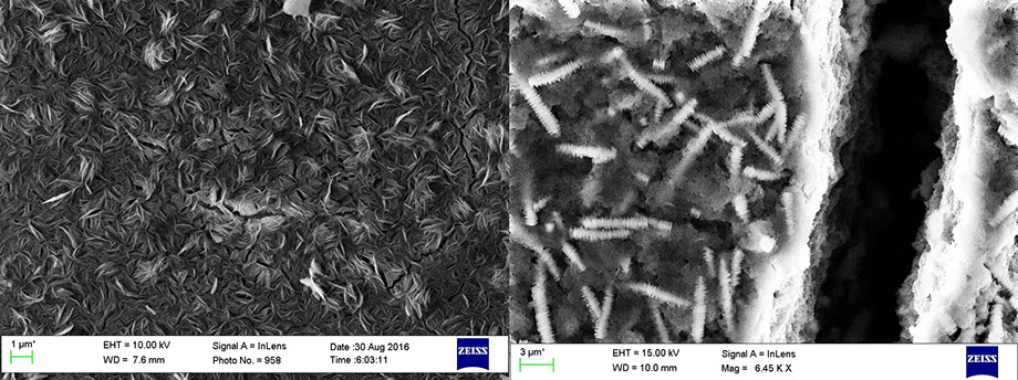
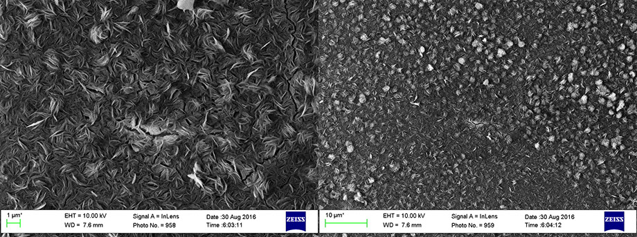
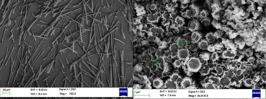
Zinc oxide (ZnO) nanorod is a one dimensional semiconductor material belonging to the II-VI group. ZnO normally crystallizes in the wurtzite structure which is non-centrosymmetric. However, as it has good electromechanical coupling, the piezoelectric and pyroelectric properties are excellent and consequently ZnO is widely used in mechanical actuators and piezoelectric sensors. ZnO has a wide and direct band gap of 3.37 eV at 300 K and a piezoelectric coefficient (d33) of 10 pm/V. There are several methods commonly used for the growth of ZnO nanorods including chemical vapour deposition (CVD), electrochemical deposition (ED), vapour-liquid-solid (VLS) growth, and metal-organic chemical vapour deposition (MOCVD). All of the aforementioned methods require high temperatures (> 500 ℃) and sophisticated equipment. In contrast, the regular hydrothermal method, though it takes more time (4 to 6 hours as compared to minutes), uses low temperatures and requires cheaper equipment. Our research focuses on the growth of ZnO nanorods through a microwave assisted hydrothermal method which is an ultra-fast technique that can produce various ZnO hierarchical nanostructures of various shapes possessing high piezoelectric coefficients. This allows us to then explore their potential applications in pressure devices.
Vertical ZnO Nanorods by Microwave-assisted growth
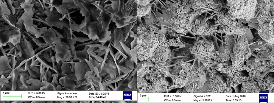
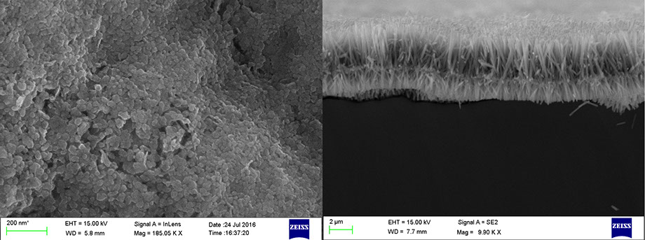
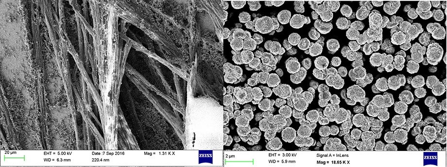
Aluminum Nitride (AlN) is group III-V material with many remarkable properties like high piezoelectricity, high ultrasonic velocity (12,350 m/s and 6,000 m/s for bulk and surface waves, respectively), high-temperature stability and stable chemical properties. Currently, we are working on deposition of AlN thin films on metal electrode/SOI stack using DC magnetron sputtering. AlN deposited by this technique is then used as piezoelectric layer for MEMS devices like PMUTs, Energy harvesters, Resonator etc. We are studying the stresses genereated during deposition by making PMUTs.
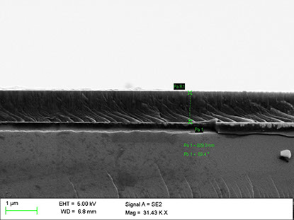
Cross section image of AlN growth on platinum
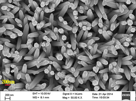
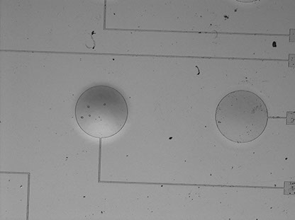
PMUT diaphragm fabricate with stressed AlN film.
MEMS Lab, Centre for Nano Science and Engineering, Indian Institute of Science. Bangalore-560012
Phone: +91 (80) 2293 3250, +91 (80) 2360 8659 Fax: +91 (80) 2360 1648 Email: pratap@iisc.ac.in, memslab@iisc.ac.in