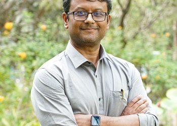
Sorry, you need to enable JavaScript to visit this website.
office.cense@iisc.ac.in | +91-80-2293 3276/ +91-80-2293 3291 | Sitemap

The Centre for Nano Science and Engineering (CeNSE) was established in 2010 to pursue interdisciplinary research on the nanoscale. Topics of interest include, but not limited to materials, electronics, MEMS/NEMS, photonics, biotechnology, and solar cells. If you have an exciting and revolutionary idea, come talk to us. We welcome both academic and industry collaborations.

CeNSE houses a state-of-the art national nanofabrication centre (NNfC) with 14000 square feet of class 100/1000 clean room. It also houses a comprehensive micro nano characterization facility (MNCF) to conduct virtually any type of electrical, optical, mechanical and material characterization. Both of these are national user facilities are accessible to outside researchers for very reasonable charges.

CeNSE faculty has 15 core members and more than 40 associate members from various IISc departments. The CeNSE family also includes 142 students, around 25 project associates, 55 technical staff, and 29 support staff. We also host over 150 researchers from outside academic institutions, governmental and industrial research labs every year, so that they can use our facilities.

The centre offers PhD and M.Tech programs in Nanoelectronics.

Prof. Srinivasan RaghavanWelcome to the Centre for Nano Science and Engineering. CeNSE, as we call ourselves, is home to an exciting group of people working on a range of interdisciplinary problems, with little regard to the background we may have come from. An aeronautical engineer works on DNA sequencing and bacterial swarms. Physicists work on nanomotors that can travel through the human body, quantum sensing, liquid helium and lasers that can blast through walls. Metallurgists work on systems at the edge of chaos, engineering atomically thin materials, developing materials for e-vehicles and 5G electronics. Electronics engineers work on sensors that analyze breath and blood, cutting edge photovoltaics, quantum communication, neuromorphic devices and integrated photonics. Mechanical engineers work on micro and nano-systems, designing speakers that mimic the noisy cricket, studying turmeric, energy dissipation and droplet formation… and of course they all work with each other.

We are supported by state-of-the-art facilities – for fabrication and characterization of micro and nanostructures- that are amongst the best in the world and managed by professional staff members. These are national facilities that can be accessed by anybody in India – students, academics, the strategic sector and industry – or for that matter, the world, through our INUP and ISTEM portals.

Science to Systems to Society is our motto. We have developed technologies based on the science we do and translated them to society either through the start-ups we have incubated, licensing to industry or transferring to the strategic sector. The Technology Business Incubator (TBI at CeNSE) has been set up to enable start-ups, from IISc and outside, that can leverage our facilities. An Industry Affiliate Program (IAP) serves as a platform to engage with industry.

Our students make us proud by excelling on the international stage, and as alumni, they have gone on to occupy exciting positions in academia, industry, start-ups and the government.

To the student out there interested in doing research, you will not find a better place than CeNSE. To the interested faculty candidate, we welcome all backgrounds. We are especially looking for women faculty candidates. To industry, come and leverage our capabilities – intellectual and infrastructural- to meet your requirements.

Regardless of your background, your interest is most welcome.

— Srinivasan Raghavan


The centre has been built around two central facilities – The National Nanofabrication Centre (NNfC) and the Micro and Nano Characterization facility (MNCF). Both are national user facilities, i.e. they are accessible to outside academic and industrial users.

Supporting the central facilities are the MEMS and IC Packaging lab, the Computational Nanoengineering (CoNe) laboratory, Systems Lab, and 14 other functionally distinct laboratories managed by various research groups. In keeping with Centre’s collaborative and open atmosphere, access to these laboratories can also be provided after appropriate permissions. For details please visit Research Facilities. Centre also houses a range of academic and recreational facilities for students and faculty.

National Nanofabrication (NNfC) 

National Nanofabrication Centre consisting of a comprehensive 14,000 sq. ft. clean-room facility with capability for:

  • Photolithography with resolution of 1 µm for optical and 10 nm for e-beam lithography.
  • Developing unit processes for chemical & physical vapour deposition (CVD) of most commonly used semiconductors and dielectrics, such as Si, SiGe, Ge, SiO2, SiNx, Al2O3, TiO2, etc.
  • Developing unit processes for wet and dry etching of most commonly used semiconductors and dielectrics.
  • Fabricating complete MEMS sensors, gas sensors, GaN HEMTs, Si solar cells, novel 1D and 2D devices including graphene and MoS2, and photonic circuits.
  • Developing new and customized processes for MEMS/NEMS devices, microfluidic structures, and semiconductor devices for industries and other laboratories.
  • Inline characterization using various metrology tools.

For more details on Nanofabrication facilities, click here.

Micro and Nano Characterization Facility (MNCF) 

The one of its kind micro and nano characterization facility (MNCF) aims to be a single shop for all a characterization needs of any nanofabrication process. It is rare to find such a comprehensive array of tools under a single roof, anywhere in the world. Capabilities include:

  • Complete electrical characterization of devices from DC to 110 MHz and at 4K to 400K temperature, using an array of probe stations and parameter analysers.
  • Ability to characterize RF devices up 70 GHz.
  • Ability to measure power conversion efficiency and external quantum efficiency (EQE) of solar cells.
  • Metrology of thin-films using optical profilometer; acoustic microscopy; and atomic force microscope (AFM), including advanced modes such as piezo response, conductive, magnetic-force, scanning-tunnelling atomic force microscopy, etc.
  • Comprehensive characterization of bulk materials and thin-films using Raman; photoluminescence (PL); electroluminescence (EL); Fourier transform infrared spectrometry (FTIR); X-ray diffraction (XRD); X-ray reflection (XRR), photoemission spectrometry (UPS and XPS); and UV-Visible spectrometery.
  • Field-emission scanning electron microscopy (FESEM) with dual beam focused ion-beam (FIB), EDS and monochrometer (MonoCL).

For more details on characterization facilities, click here.

Systems & Packaging Facility

Systems Engineering is an ESD safe workspace which houses various electronic test & measurement equipments, ESD work stations, soldering and desoldering stations, PCB design tool, embedded and software design tools, pressure sensor calibration setup, particulate matter counter, various gas & pressure sensors, electronic modules & components and processors' based evaluation kits,

MEMS and IC Packaging facility has the complete capability to convert a wafer into a packaged device – from wafer sawing to wire bonding to precision welding. In addition, there are dedicated setups for pneumatic/hydraulic pressure calibration for pressure sensors and acoustic calibration for acoustic sensors. For more details on Systems and Packaging facilities, click here

Computational Facility

Computational Nanoengineering (CoNe) laboratory has 24 computers with Windows and Unix operating systems for simulations and modelling. It also houses CeNSE mail, web, and data backup servers. The lab is currently engaged in developing a simulation module for microsystems and integrating in a commercial finite element software, NISA. Also pursued in the lab are projects in algorithms for simulation and scientific computing including graphical processor unit (GPU) based computing. Commercial modelling packages such as Matlab, Synopsys, Sentaurus, etc. are available for use.

Library

CeNSE maintains a growing library of books on nanoscience. The access to books is provided to all Centre members free of charge. Library has a committed yearly budget and both students and faculty can request titles for purchase. The library is open for weekday from 3pm to 5pm.

Café

The Café functions as the social hot-spot of CeNSE. With an open layout that connects to the scenic balcony, Café is the perfect spot to take a break. It is cozy enough to catch up with friends over a game of chess and spacious enough for some quiet introspection as you watch the setting sun. Menu includes light refreshments and beverages.

Student Offices

CeNSE is one of the few department that have dedicated office spaces for all PhD students. The goal is to encourage student-to-student interaction away from the hectic hustle of labs and eyes of the faculty. All students sit in air-conditioned halls with modern & spacious cubicles that balance the twin needs of proximity and privacy.

M.Tech. Lounge

M.Tech. students enjoy the unique privilege of a dedicated lounge. The lounge is perfect for group study sessions (right before assignment deadline!), study or just relaxing on the couch with a beautiful view of the campus. For convenience, computers and personal lockers are provided.

Faculty Lounge

Currently under construction, the lounge will also house a mini gym where members can sweat it out between experiments.

Sports Courtyard

The CeNSE backyard doubles up as sports arena perfect for some badminton, volleyball, or gully cricket. Because there is no safer way to beat your adviser than a racket!


.

Address

Chairman
Centre for Nano Science and Engineering (CeNSE)
Indian Institute of Science, Bangalore – 560012, Karnataka,
India.

Office

Dr. R. N. Narahari (PhD)
Phone: +91-80-2293 3276, +91-80-2293
Fax: +91-80-2360 4656
Email: office.cense@iisc.ac.in

Indian Institute of Science is located in Mathikere, Bangalore. The locals refer to IISc as ‘Tata Institute’, so it may be more helpful to use ‘Tata Institute’ with the taxi, auto drivers, and bus conductors. The main gate of the IISc is at its southern end, on C.V. Raman Road that connects Yeshwathpura to Mekhri circle. From the IISc main gate, CeNSE is ~1 km to the north. The campus can also be accessed from the east, via “Ramaiah gate” on the BEL road. The most convenient is Gate ‘D’ on M. S. Ramaiah road, which is on the western side of the campus.

In terms of neighbourhoods, to the north of the campus is Malleshwaram, to the east is Ashwath Nagar, to the west is Subedarpalya, and to the south Mathikere. Landmarks are Ramaiah Medical College on the south, Kendriya Vidyalaya on the west, Central Power Research Institute (CPRI) to the east, and BHEL on the north.

From the Airport

Tata Institute (IISc) is about 30 km south from the Bangalore Airport (both domestic and international). Taxis (~800-900/-) and BMTC Airport Shuttle (~250/-) are available at the airport to IISc.

From the Bangalore City Railway Station

Bangalore is connected to all major Indian cities by rail. The City Railway Station is the main terminal in Bangalore, which is about 7 km south of the IISc campus. You should get out towards platform number ONE. From there you can hire a prepaid city taxi (costs ~ Rs. 150), or a prepaid Auto (costs ~ Rs. 40). Alternatively, walk to Kempegowda bus station (popularly called “Majestic”) and take one of the many buses to “Divanarapalya”– route numbers 269, 269B, 271D, 271G, 271K, 273, 273B, 273F, 275C, etc. Gate D is walking distance from Divanarapalya.

From the Cantonment Railway Station

Cantonment Railway Station is the second major railway station in Bangalore, popularly called Bangalore Cantt. It is also about 7km from IISc. The distance from this station to IISc is almost same as the Bangalore City railway station and it also has prepaid taxi and auto facility. Alternatively, walk to Vasantha Nagar Ambedkar Bhavan BMTC bus stop. Take the bus to “Tata Institute” – route numbers 94E, 252A, 270E,G-8, and K-1. IISc main gate is right next to the Tata Institute bus stop.

From the Yeshwanthpura Railway Station

The third railway station in Bangalore, also the closest to IISc, is Yeshwanthapura. The station is less than 3 km from IISc. It has a prepaid stand. Alternatively, take bus 401BR to “Divanarapalya” and walk to Gate D.

From the Kempegowda Bus Station

The KBS is right opposite the City Railway Station. Commonly known as Majestic, is about 7 km from IISc. Take one of the many buses to “Divanarapalya”– route numbers 269, 269B, 271D, 271G, 271K, 273, 273B, 273F, 275C, etc. Gate D is walking distance from Divanarapalya.

From any other part of Bangalore

You can hire a taxi or an auto from any part of the city. Auto fare between 10:00 p.m. and 06:00 a.m. will cost 50% more.