
RESEARCH BREAKTHROUGHS
 |
REVERSIBLE OXYGEN MIGRATION AND PHASE TRANSITIONS IN HAFNIA_BASED FERROELECTRIC DEVICES |
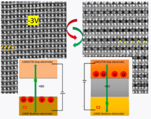
Hafnia-based materials are of interest because of their potential use in microelectronic components. Hafnia-oxide is a ferroelectric material, but whether the polarization switching comes from the polar crystal phases or the migration of oxygen vacancies has remained an open question. Nukala et al. attempted to resolve this controversy by conducting electron microscopy during the operation of a hafnium zirconium oxide capacitor.
Unconventional ferroelectricity exhibited by hafnia-based thin films—robust at nanoscale sizes—presents tremendous opportunities in nanoelectronics. However, the exact nature of polarization switching remains controversial. We investigated a La0.67Sr0.33MnO3/Hf0.5Zr0.5O2 capacitor interfaced with various top electrodes while performing in situ electrical biasing using atomic-resolution microscopy with direct oxygen imaging as well as with synchrotron nanobeam diffraction. When the top electrode is oxygen reactive, we observe reversible oxygen vacancy migration with electrodes as the source and sink of oxygen and the dielectric layer acting as a fast conduit at millisecond time scales. With nonreactive top electrodes and at longer time scales (seconds), the dielectric layer also acts as an oxygen source and sink. Our results show that ferroelectricity in hafnia-based thin films is unmistakably intertwined with oxygen voltammetry.
 |
DROP
|
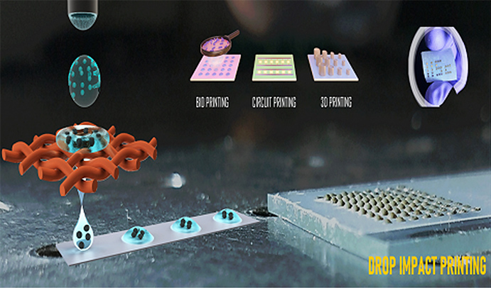
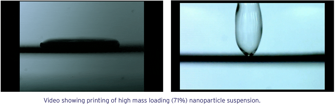
Pursuit to accurately print microscale droplets is not new. However, with the advent of additive manufacturing and 3D bio-printing, research interest in this technology has been renewed. Newer applications demand use of inks which are not well suited for conventional printers. For example, bio-printing requires dispensing live cells. Viability of cells is dramatically reduced by the thermal or piezoelectric actuation used in conventional printers. Further, printing inks with higher mass loading (i.e. larger quantity of particles or cells per droplet) is desirable and often necessary. This remains a challenge which has not been addressed till date. Printers employ a nozzle with small orifice to form the droplets. Particles in inks with high mass loading have a tendency to aggregate at the orifice causing the nozzle to clog.
The technique in this study addresses these problems by replacing the nozzle with a mesh. Nanowires are grown on the mesh and the nanostructured surface of the mesh is chemically treated to render it superhydrophobic. When a large droplet (2-3 mm in diameter) driven by gravity, impacts the super hydrophobic mesh, it is repelled by the non-wetting surface and the droplet bounces back. However, during this droplet rebound an interesting phenomenon takes place. As the droplet spreads upon impact, a cavity is formed at the centre of the impacting droplet. During the recoil phase of the impact this cavity collapses, leading to a singularity. The kinetic energy of the recoiling interface gets focused and this leads to ejection of a single satellite-free microscale droplet. The size of the generated droplets depends on the pore opening of the mesh. The generation of droplets ranging from 40 microns to 960 microns in diameter has been demonstrated here. Capability to disperse such a large range of droplet sizes is unique to this technique.
Image Credit: Nature communications, Microfluidic Devices & Heterogeneous Systems Lab, CeNSE, IISc Bangalore.
Video: https://www.youtube.com/watch?v=TCmkuCFR4Go
The paper “Modak, C.D., Kumar, A., Tripathy, A. et al. Drop impact printing. Nature Communications 11, 4327 (2020) can be accessed here: https://doi.org/10.1038/s41467-020-18103-6.