Sorry, you need to enable JavaScript to visit this website.
office.cense@iisc.ac.in | +91-80-2293 3276/ +91-80-2293 3291 | Sitemap

TECHNOLOGY DEVELOPMENT

Double-peak signal features in microfluidic impedance flow cytometry enable sensitive measurement of cell membrane capacitance

In a microfluidic impedance cytometer with co-planar microelectrodes, unusual “double peak” features were observed in the reactive component of the electrical signatures from individual red blood cells. This phenomenon was observed only at specific frequencies (400 - 800 kHz) and its occurrence was facilitated by the microelectrode geometry.

NANOMOTORS PROBING TUMOR MICROENVIRONMENT

In this work the team of researchers steered helical nanomotors remotely, via an external magnetic field, through a tumour model to sense, map and quantify changes in the cellular environment. The model comprises both healthy and cancer cells embedded within a reconstituted basement membrane matrix and mimics the breast cancer environment.

GATE TUNABLE COOPERATIVITY BETWEEN VIBRATIONAL MODES

Coupling between a mechanical resonator and optical cavities, microwave resonators, or other mechanical resonators have been used to observe interesting effects from sideband cooling to coherent manipulation of phonons. Here we demonstrate strong coupling between different vibrational modes of MoS2 drum resonators at room temperature. We observe intermodal as well as intramodal coupling.

A NEW ‘‘TWEEZER IN A TWEEZER” TECHNOLOGY

Manipulation of colloidal objects with light is important in diverse fields. While performance of traditional optical tweezers is restricted by the diffraction-limit, recent approaches based on plasmonic tweezers allow higher trapping efficiency at lower optical powers but suffer from the disadvantage that plasmonic nanostructures are fixed in space, which limits the speed and versatility of the trapping process.

ANTI-MICROBIAL SURFACES

Antimicrobial-resistant infections currently claim 700,000 lives each year from across the world and this figure will increase alarmingly to 10 million by 2050 if it is not stopped. One of the methods to tackle biofilms involves prevention of biofilm formation by actively killing the bacteria as soon as they arrive on the surface.

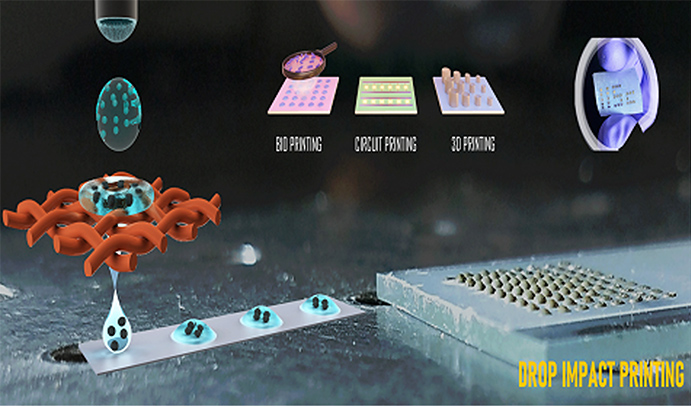
DROP IMPACT PRINTING

Pursuit to accurately print microscale droplets is not new. However, with the advent of additive manufacturing and 3D bio-printing, research interest in this technology has been renewed. Newer applications demand use of inks which are not well suited for conventional printers. For example, bio-printing requires dispensing live cells. Viability of cells is dramatically reduced by the thermal or piezoelectric actuation used in conventional printers.

NANOROBOTS AS MOBILE NANOTWEEZERS

Controlled manipulation of nanoscale objects in fluidic media is one of the defining goals of modern nanotechnology. So far, plasmonic tweezers – nanosized tweezers made up of noble metals -- are used to trap such small sized cargo.

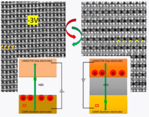
BREAKING THE BOLTZMANN LIMIT FOR LOW POWER NANO-TRANSISTOR

Power consumption in modern electronic devices is a major technological and environmental concern. This is because although technologists are able to reduce the dimensions of the transistor, they are unable to reduce the voltage required for its operation (called supply voltage).

Development of a novel vapor-annealing process to consistently and reliably get high-performance perovskite solar cells

Spin coated perovskite thin films are known to poor device-to-device repeatability, mostly due to poor control on morphology of the deposited films. In this work, a post-deposition vapor annealing process was developed, which “fixes” the issues with as-deposited films, leading to high-efficiency perovskite solar cells with excellent repeatability (standard deviation of only 0.7%).

Fate of an Intruder in Colloidal Nanocrystals is Governed by Entropy

Using a modified and highly configurable optical trap we have observed formation of 2D colloidal crystallites whose phase and sizes can be controlled. This system allows us to study the dynamics of foreign dopants injected into the crystallites. The striking result obtained here was the ability of finite-sized colloidal clusters to expel or internalize a foreign dopant depending on its initial position.

NEMS Lab / Micro and Nano Sensors Lab

The Micro and Nano Sensors Lab focuses on physics and applications of Nanoelectromechanical Systems (NEMS). Activities of this lab include fabrication of resonant NEMS devices with frequencies in VHF and UHF ranges, novel actuation and detection schemes at these frequencies and nano-dimensions, study of noise processes that govern the frequency stability of these ultra-sensitive devices and their utility in various applications including NEMS mass spectrometery and gas sensing. Facilities include a NEMS-based mass spectrometery system, two closed cycle cryostats capable of reaching below 10K, an ultra-high vacuum system to probe frequency noise in NEMS devices and electrical characterization equipment including spectrum analyzers and microwave signal sources.

Bio Sensors Lab

Focuses on developing low-cost biosensors for various bioanalytes of interest. Involves study of various surface modification methodologies. Facilities include electrochemical workstation, chemical synthesis equipment, equipment for processing biomolecules.

MEMS/MOEMS Lab

Design and development of MEMS inertial sensors, MEMS microphones, capacitive and peizoelectric ultrasound transducers (CMUTs and PMUTs), suspended gate FET-coupled MEMS sensors, all-optical actuation and sensing MEMS, study of energy dissipation in micro and nanoscale structural vibrations, study of microscale biosensors in insects, haltere dynamics, and cell dynamics. Facilities include experimental measurement tools for subnanoscale vibrations, angular rate measurements, ultrasound transmitters and receivers, and optical imaging, including high speed videography.

Biophotonics and Bioengineering

Our work follows two themes. One is the development of sensors to sense various molecules (molecular sensors) for bio/chemical applications and the other is to understand the molecular sensing process in terms of robustness to interference or perturbation. The robustness often emerges as a consequence of complexity in sensor design and/or in sensory signal processing. Examples of complexity in sensor design could be our olfactory receptors which enable our sense of smell or the signalling cascades employed by immune cells in our body to identify infective pathogens. We are interested in understanding the performance limits of molecular sensing, i.e. limits of sensitivity, accuracy, tolerance to interference and so on.

Optics, Nanostructures and Quantum Fluids

Study of optical and hydrodynamic properties of nanostructured particles and films, with emphasis on developing nanoscale drug delivery vehicles and nanoplasmonic sensors for biological applications. Facilities include nanostructured thin film fabrication system, optical microscope, and various optical characterization tools.

Gas Sensors Lab

The Lab has facilities to characterize sensors employing different concentrations of gases – both inorganic and volatile organics – from ppb (~1) to ppm (>10,000); an IR camera to study the thermal morphology of microheaters; a microdispenser to dispense a desired amount of an analyte (solution) with a 20 μm spatial resolution. The lab also has the facility to fabricate sputtering targets of sensor materials.

Functional Thin Films Lab

The lab conducts investigations on influence of process parameters on the structure and properties of functional thin films, leading to the development of micro and nano sensors and actuators. Faciltiies include evaporation, sputtering and ion beam systems, designed and fabricated for specific requirements.

Photovoltaics and Energy Lab

The lab is primarily designed to fabricate various types of photovoltaic devices. The lab also shares the workload of the National Nano Fabrication Facility.

Polymer Process Lab

The lab specializes in microwavebased chemical synthesis, wet-etching, chemical processing, electrochemical characterization, organic electronics, and thin-film batteries.

Non-linear Photonics and High Power Lasers Lab

This laboratory focuses on development of novel optical sources and processing technologies for varied applications from optical communications, sensing and biomedical imaging to high power industrial and defense lasers. Fundamental research on non-linear optics in guided-wave devices, an enabler for many of the novel laser technologies, is also undertaken.

Neuro-Electronics Lab

The research emphasis is on interfacing neurons of the brain with electronic devices. The broad aim is to understand how learning takes place in biological neuronal networks using electrical and optical recording and stimulation, and to utilize it for robotic control. Facilities available are: nanofabrication of multi-electrode arrays, tissue culture laboratory for neuronal culture, electrophysiology rigs for multi-electrode array recording with feedback control, an electronics lab bench, high-end microscopes with fast fluorescence imaging and optical stimulation of neurons using a femto-second laser.

Heterojunction Lab

This laboratory conducts research in design, fabrication and characterization of novel electronic devices. The focus is on integrating different semiconductor materials with each other, e.g. silicon with metal-oxides or germanium to silicon. Such heterogenous integration introduces novel functionality and improves performance for the next generation of electronic devices.

Photonics

Photonics Research Laboratory is a dedicated characterization facility for integrated photonic devices and circuits. The primary focus of the lab is to develop high-speed integrated photonic devices for next-generation computing and communication. The lab houses a comprehensive high-speed electro-optic testbed for characterizing bandwidth of discrete devices such as Wavelength filters, light modulators, photodetectors, and amplifiers in the O, C, and L bands. The device and circuits developed are tested using a custom developed vertical and horizontal optical probe station. Research in the lab is also aimed at exploiting the photonic circuit for on-chip gas and biosensors. Spectrometers spanning from visible to Near-IR are used to develop such on-chip sensors.

A key goal at CeNSE is to drive the development of technology from advances in science and engineering research carried out in the department. Being a young department, this effort is still in nascent stages, however, there have already been several examples and in this page we list a few of them.

2024

  1. Sharma KSandeep, TS ARaman, Pillai G, . Temperature and Bias-Dependent Switchability and Tuneability of Very High-Quality Factor GHz Resonators. In 2024 IEEE 37th International Conference on Micro Electro Mechanical Systems (MEMS). IEEE; 2024.
  2. Goswami A, Dash S, Deheri R, Supradeepa VR. Widely tunable visible pulsed cascaded Raman fiber laser source. In Nonlinear Frequency Generation and Conversion: Materials and Devices XXIII [Internet]. SPIE; 2024. https://doi.org/10.1117/12.3000916
  3. Javed N, Kumar A, Tiwari S, Pratap R, Pillai G. Dummy device-based feedthrough cancellation for PZT on Silicon microcantilever for viscosity sensing. In 2024 8th IEEE Electron Devices Technology & Manufacturing Conference (EDTM). IEEE; 2024.
  4. Dash S, Deheri R, Supradeepa VR. Linewidth control of cascaded Raman fiber lasers and visible conversion. In Fiber Lasers XXI: Technology and Systems [Internet]. SPIE; 2024. https://doi.org/10.1117/12.3002546
  5. Lakshmi CG, Supradeepa VR. A novel detection mechanism for nonlinear distortions in ultrashort pulses transmitted through dynamic fiber optic links. In Frontiers in Ultrafast Optics: Biomedical, Scientific, and Industrial Applications XXIV [Internet]. SPIE; 2024. https://doi.org/10.1117/12.3000816
  6. Kumar P, Sahana D, Chandrashekar LN, Jeyaseelan A, Nayak MM, Pratap R, et al. A Wide-Range Resonant Pressure Sensor With Enhanced Sensitivity Based On An Indirect Coupling Scheme. In 2024 IEEE 37th International Conference on Micro Electro Mechanical Systems (MEMS). IEEE; 2024.
  7. Jain P, Gupta G, Kwon H-K, Vukasin GD, Chandorkar SA. Machine Learning Based Nonlinear Resonator System Identification. In 2024 IEEE 37th International Conference on Micro Electro Mechanical Systems (MEMS). IEEE; 2024.
  8. Dash S, Goswami A, Deheri R, Avasthi S, Supradeepa VR. Multi-point thermal monitoring of silicon wafer under processing utilizing a spectrally shaped supercontinuum source. In High-Power Laser Materials Processing: Applications, Diagnostics, and Systems XIII [Internet]. SPIE; 2024. https://doi.org/10.1117/12.3002717
  9. Dash RK, Selvaraja SKumar. Passive wavelength selective polarization rotator in a hybrid waveguide platform. Optics Express [Internet]. 2024;32:13035–13047. https://doi.org/10.1364/OE.515141
  10. Dash RK, Selvaraja SKumar. Sandwiched hybrid waveguide platform for integrated photonics application. Optics Communications [Internet]. 2024;550:129959. https://doi.org/10.1016/j.optcom.2023.129959
  11. Paramanick A, Roy K, Paul S, Kumar A, Ashok A, Pratap R, et al. Seeing Beyond: The Future of Photoacoustic Imaging with Single-element, Low-frequency Thin-film PMUT. IEEE Sensors Letters. 2024;.
  12. Khandelwal U, Sandilya RSatya, Rai RKumar, Sharma D, Mahapatra SRekha, Mondal D, et al. Large electro-opto-mechanical coupling in VO2 neuristors. Applied Physics Reviews [Internet]. 2024;11. https://doi.org/10.1063/5.0169859
  13. Arora N, Singh P, Kumar R, Pratap R, Naik A. Mixed Nonlinear Response and Transition of Nonlinearity in a Piezoelectric Membrane. ACS Applied Electronic Materials [Internet]. 2024;6:155–162. https://doi.org/10.1021/acsaelm.3c00735
  14. Lathia R, Deshmukh P, Vinaya V, Sen P. Coalescence of liquid marbles on oil-infused surface. Physics of Fluids [Internet]. 2024;36. https://doi.org/10.1063/5.0196769

2023

  1. Paramanick A, Roy K, Samanta D, Aiswarya KS, Pratap R, M Singh S. Image quality enhancement of PMUT-based photoacoustic imaging. In Photons Plus Ultrasound: Imaging and Sensing 2023 [Internet]. SPIE; 2023. https://doi.org/10.1117/12.2650488
  2. Reddy BSankar, Modak CDey, Lathia R, Agarwal B, Sen P, . Direct Patterning on Porous Surface Using Drop Impact Printing. In 2023 IEEE 36th International Conference on Micro Electro Mechanical Systems (MEMS). IEEE; 2023.
  3. Lathia R, Reddy BSankar, Modak CDey, Nagpal S, Sen P. Temperature-Responsive Microcapsules Manufactured by Promoting Controlled Cloaking with the Help of Micro/Nanoparticles. In 2023 IEEE 36th International Conference on Micro Electro Mechanical Systems (MEMS). IEEE; 2023.
  4. Baby R, Reshma K, Chandrasekar H, Muralidharan R, Raghavan S, Nath DN. Study of TaN-gated p-GaN E-mode HEMT. IEEE Transactions on Electron Devices. 2023;70:1607–1612.
  5. Lathia R, Nampoothiri KNarayanan, Sagar N, Bansal S, Modak CDey, Sen P. Advances in Microscale Droplet Generation and Manipulation. Langmuir [Internet]. 2023;. https://doi.org/10.1021/acs.langmuir.2c02905
  6. Gowrisankar A, Charan VSai, Chandrasekar H, Venugopalarao A, Muralidharan R, Raghavan S, et al. Compensation Dopant-Free GaN-on-Si HEMTs With a Polarization Engineered Buffer for RF Applications. IEEE Transactions on Electron Devices. 2023;.
  7. Pradhan D, Neeramoole S, Yadav N, Ghosh A. Using a cylindrical piezoelectric transducer to focus ultrasound in superfluid helium. The European Physical Journal Special Topics. 2023;:1–7.
  8. Nukala P, Rao A, Sanjay S, Ahmadi M, Venugopalrao A, Bhat N, et al. Realizing neuromorphic networks at self-organized criticality on a 2D hexagonal BN platform. [Internet]. 2023;. https://doi.org/10.21203/rs.3.rs-2405755/v1
  9. Bhosale KS, Zope AA, Pillai G, Li S-S. Tiny-Gap Titanium-Nitride-Composite MEMS Resonator Designs With High Power Handling Capability. Journal of Microelectromechanical Systems. 2023;.

2022

  1. Rathkanthiwar S, Nath D, Raghavan S, Selvaraja SKumar, . GaN-on-Sapphire Photonic Circuit with Polarization Independent Grating Coupler at 1550 nm. In Integrated Photonics Research, Silicon and Nanophotonics. Optica Publishing Group; 2022.
  2. Chang C-Y, Pillai G, Li S-S. Phase Noise Optimization of Piezoelectric Bulk Mode MEMS Oscillators Based on Phase Feedback in Secondary Loop. In 2022 IEEE 35th International Conference on Micro Electro Mechanical Systems Conference (MEMS). IEEE; 2022.
  3. P MSajeer, Varma MM. Exploring electric field sensing for solid-state nanopores. arXiv e-prints. 2022;:arXiv–2210.
  4. Yarajena SSaraswathi, Naik AK. Nano Flex Screen Protectors for 2D Material Piezotronics. IEEE Transactions on Nanotechnology. 2022;.
  5. Choudhury S, Joshi A, Dasgupta D, Ghosh A, Asthana S, Chatterjee K. 4D Printed Biocompatible Magnetic Composite for Minimally Invasive Deployable Structures. 2022;.
  6. Rao A, Sanjay S, Ahmadi M, Venugopalrao A, Bhat N, Kooi B, et al. Self-assembled neuromorphic networks at self-organized criticality in Ag-hBN platform. arXiv preprint arXiv:2301.01619 [Internet]. 2022;. https://doi.org/10.48550/arXiv.2301.01619
  7. Roy K, Paramanik A, Paul S, Kalyan A, Sarkar E, Ashok A, et al. Photoacoustic Image Quality Improvement from a Single Cell Low Frequency PMUT. arXiv preprint arXiv:2211.17145 [Internet]. 2022;. https://doi.org/10.48550/arXiv.2211.17145
  8. Sharma KSandeep, Jen H-T, Li S-S, Pillai G. Investigation of support transducer enabled higher-order radial bulk mode MEMS resonator and low phase noise oscillator. Journal of Micromechanics and Microengineering. 2022;32:084004.
  9. Prakash P, Varma M. A Pedagogical Introduction to Biomarker Detection in Surface-Based Biosensors. Journal of Chemical Education [Internet]. 2022;99:3694–3701. https://doi.org/10.1021/acs.jchemed.2c00606
  10. Patil G, Ghosh A. Analysing the motion of scallop-like swimmers in a noisy environment. The European Physical Journal Special Topics. 2022;:1–7.
  11. Shastri V, Majumder S, Ashok A, Roy K, Pratap R, Kumar P. Electric current-assisted manipulation of liquid metals using a stylus at micro-and nano-scales. Nanotechnology. 2022;.
  12. Suri P, Deshpande P, Ghosh A. Characterization of monolayer WSe2 sandwiched in a hetero-plasmonic dimer. Nano Express. 2022;3:045001.
  13. Lathia R, Sen P. Sol-gel-derived nanoparticles coated liquid entities: liquid marbles, liquid plasticine, and flat interface. Journal of Micromechanics and Microengineering. 2022;.
  14. Li S-S, Ganesh RHosur, Pillai G, Chien-Hao WENG. Acceleration sensing structure and accelerometer. 2022.

2021

  1. Sharma A, Bhargav G, Kaushal A, Bhat KN, Ghosh A. Direct laser writing on silicon surface for large area nanoplasmonic devices. In Novel Patterning Technologies 2021 [Internet]. International Society for Optics and Photonics; 2021. https://doi.org/10.1117/12.2583823
  2. Prakash R, Vikram BS, Supradeepa VR. Polarization maintaining, narrow linewidth fiber laser with> 1kW output power using a novel dual sine and noise modulation for enhanced SBS suppression. In Fiber Lasers XVIII: Technology and Systems [Internet]. International Society for Optics and Photonics; 2021. https://doi.org/10.1117/12.2583154
  3. Saini TSingh, Arora S, Supradeepa VR. Mid-infrared wavelength conversion using a composite Si3N4-HfO2 waveguide device. In Integrated Optics: Devices, Materials, and Technologies XXV [Internet]. International Society for Optics and Photonics; 2021. https://doi.org/10.1117/12.2582755
  4. Roy K, Kalyan K, Ashok A, Shastri V, Pratap R. Development of Frequency Tunable Fluid Loaded PMUTs. In 2021 IEEE International Ultrasonics Symposium (IUS) [Internet]. IEEE; 2021. 10.1109/IUS52206.2021.9593352
  5. Roy K, Kalyan K, Ashok A, Shastri V, Pratap R. A Pmut Integrated Microfluidic System for Volumetric Flow Rate Sensing. In 2021 21st International Conference on Solid-State Sensors, Actuators and Microsystems (Transducers). IEEE; 2021.
  6. Singh S, Selvaraja SKumar. Sputter-deposited PZT-on-Silicon electro-optic modulator. In 2021 IEEE Photonics Conference (IPC). IEEE; 2021.
  7. Singh J, Sharma V, Chandorkar S, Sen P. Bacterial Force on Nanopillars: Interaction at Single Cell. In 2021 21st International Conference on Solid-State Sensors, Actuators and Microsystems (Transducers). IEEE; 2021.
  8. Roy K, Ashok A, Kalyan K, Shastri V, Jeyaseelan A, Nayak MM, et al. Towards the development of backing layer for piezoelectric micromachined ultrasound transducers. In Photons Plus Ultrasound: Imaging and Sensing 2021 [Internet]. International Society for Optics and Photonics; 2021. https://doi.org/10.1117/12.2582504
  9. Kallega R, Shekhawat R, Udaya RK, Kuruppannan R, Selvaraja SKumar. Controlled phase change of GST-on-SOI for photonic neuromorphic application. In 2021 IEEE Photonics Conference (IPC). IEEE; 2021.
  10. Roy K, Thomas A, Paul S, Ashok A, Shastri V, Kalyan K, et al. An optofluidic dye concentration detector based on the pulsed photoacoustic effect. In Microfluidics, BioMEMS, and Medical Microsystems XIX [Internet]. International Society for Optics and Photonics; 2021. https://doi.org/10.1117/12.2582656
  11. Nampoothiri KNarayanan, Sen P. Motion of Generated Dumbbell-Shaped Satellite Droplets during Liquid Dielectrophoresis. Journal of Micromechanics and Microengineering. 2021;.
  12. Roy K, Kalyan K, Ashok A, Shastri V, Jeyaseelan A, Mandal A, et al. A PMUT Integrated Microfluidic System for Fluid Density Sensing. arXiv preprint arXiv:2104.11793. 2021;.
  13. Subhani KNizammuddi, Remesh N, Niranjan S, Raghavan S, Muralidharan R, Nath DN, et al. Nitrogen rich PECVD Silicon Nitride for passivation of Si and AlGaN/GaN HEMT devices. Solid-State Electronics [Internet]. 2021;:108188. https://doi.org/10.1016/j.sse.2021.108188
  14. Ramachandran RVasantha, Bhat R, Saini DKumar, Ghosh A. Theragnostic nanomotors: Successes and upcoming challenges. Wiley Interdisciplinary Reviews: Nanomedicine and Nanobiotechnology [Internet]. 2021;:e1736. https://doi.org/10.1002/wnan.1736
  15. Kalkal A, Kadian S, Kumar S, Manik G, Sen P, Kumar S, et al. Ti3C2-MXene decorated with nanostructured silver as a dual-energy acceptor for the fluorometric Neuron Specific Enolase detection. Biosensors and Bioelectronics [Internet]. 2021;:113620. https://doi.org/10.1016/j.bios.2021.113620
  16. Kumar A, Nambiar S, Kallega R, Ranganath P, Ea P, Selvaraja SKumar. High-efficiency vertical fibre-to-polymer waveguide coupling scheme for scalable polymer photonic circuits. Optics Express. 2021;29:9699–9710.
  17. Mohta N, Rao A, Remesh N, Muralidharan R, Nath DN. An artificial synaptic transistor using an α-In 2 Se 3 van der Waals ferroelectric channel for pattern recognition. RSC Advances. 2021;11:36901–36912.
  18. Sakhuja N, Jha R, Bhat N. Facile green synthesis of 2D hexagonal MoO3 for selective detection of ammonia at room temperature. Materials Science and Engineering: B [Internet]. 2021;271:115249. https://doi.org/10.1016/j.mseb.2021.115249
  19. Nayak B, Gupta H, Roy K, Ashok A, Shastri V, Pratap R. An Experimental Study of the Acoustic Field of a Single-Cell Piezoelectric Micromachined Ultrasound Transducer (PMUT). arXiv preprint arXiv:2108.04660. 2021;.
  20. Kumar V, G Saravanan S, Duraiswamy P, Selvaraja SKumar. Single Stage Low Noise Inductor-Less TIA for RF Over Fiber Communication. IEEE Access. 2021;9:141504–141512.
  21. Pradhan DKumar, Yadav N, Rath PKishore, Ghosh A. Trapping Multielectron Bubbles Using a Point Paul Trap. Journal of Low Temperature Physics. 2021;:1–8.
  22. Gupta A, Sakhuja N, Jha RKumar, Bhat N. Ultrasensitive chemiresistive humidity sensor based on gold functionalized WS2 nanosheets. Sensors and Actuators A: Physical [Internet]. 2021;331:113008. https://doi.org/10.1016/j.sna.2021.113008
  23. Yadav N, Sen P, Ghosh A. Bubbles in superfluid helium containing six and eight electrons: Soft, quantum nanomaterial. Science Advances. 2021;7:eabi7128.
  24. Kumar S, Abraham E, Kumar P, Pratap R. Introducing Water Electrolithography. ACS Omega. 2021;.
  25. Sur S, Ghosh A, Venkataraman V. Temporal coherence of surface plasmons in silver waveguides. JOSA B. 2021;38:1457–1461.
  26. Pal UM, Vishnu GKAnil, Varma M, Vaidya JS, Pandya HJ. Thermo-Optic Measurements and their Inter-Dependencies for Delineating Cancerous Breast Biopsy Tissue from Adjacent Normal. Journal of Biophotonics [Internet]. 2021;:e202100041. https://doi.org/10.1002/jbio.202100041
  27. Singh J, Hegde PB, Ravindra P, Sen P, Avasthi S. Ambient Light-Activated Antibacterial Material: Manganese Vanadium Oxide (Mn2V2O7). ACS Applied Bio Materials [Internet]. 2021;4:6903–6911. https://doi.org/10.1021/acsabm.1c00605
  28. Pahal S, Boranna R, Prashanth GR, Varma MM. Simplifying Molecular Transport in Polyelectrolyte Multilayer Thin Films. Macromolecular Chemistry and Physics [Internet]. 2021;:2100330. https://doi.org/10.1002/macp.202100330
  29. Xiao M, Carey RL, Chen H, Jiao X, Lemaur V, Schott S, et al. Charge transport physics of a unique class of rigid-rod conjugated polymers with fused-ring conjugated units linked by double carbon-carbon bonds. Science Advances. 2021;7:eabe5280.
  30. Ganapathi KLakshmi, Bhat N, Mohan S. Optimization and integration of ultrathin e-beam grown HfO2 gate dielectrics in MoS2 transistors. Journal of Physics D: Applied Physics. 2021;54:445302.
  31. Maria KHanium, Sakhuja N, Jha RKumar, Bhat N. Ultra-Sonication Assisted Synthesis of 2D SnS 2 Nanoflakes for Room-Temperature No Gas Detection. IEEE Sensors Journal. 2021;21:10420–10427.
  32. Patil G, Vashist E, Kakoty H, Behera J, Ghosh A. Magnetic nanohelices swimming in an optical bowl. Applied Physics Letters [Internet]. 2021;119:012406. https://doi.org/10.1063/5.0058848
  33. Reddy J, Chaman JJ, Pradeep K, Nayak MM, Pratap R. A method for realizing robust micro-scale electromagnetic actuators for high current density applications. ISSS Journal of Micro and Smart Systems. 2021;:1–6.
  34. Tiwari S, Kumar R, Dangi A, Dutta S, Pratap R, . Low Cost, Contamination-Free, and Damage-Free Fabrication of PZT MEMS on SOI Substrate. Journal of Micromechanics and Microengineering. 2021;.
  35. Remesh N, Chandrasekar H, Venugopalrao A, Raghavan S, Rangarajan M, Nath DN. Re-engineering transition layers in AlGaN/GaN HEMT on Si for high voltage applications. Journal of Applied Physics [Internet]. 2021;130:075702. https://doi.org/10.1063/5.0045952
  36. Dash A, More SK, Arora N, Naik AK. Ultra-sensitive charge detection and latch memory using MoS2-nanoresonator-based bifurcation amplifiers. Applied Physics Letters. 2021;118:053105.
  37. Vura S, Jeyaselvan V, Biswas R, Raghunathan V, Selvaraja SKumar, Raghavan S. Epitaxial BaTiO3 on Si (100) with In-Plane and Out-of-Plane Polarization Using a Single TiN Transition Layer. ACS Applied Electronic Materials [Internet]. 2021;. https://doi.org/10.1021/acsaelm.0c00842
  38. Nanda A, Singh V, Jha RKumar, Sinha J, Avasthi S, Bhat N. Growth-Temperature Dependent Unpassivated Oxygen Bonds Determine the Gas Sensing Abilities of Chemical Vapor Deposition-Grown CuO Thin Films. ACS Applied Materials & Interfaces [Internet]. 2021;13:21936–21943. https://doi.org/10.1021/acsami.1c01085
  39. Hassan Y, Park JHyun, Crawford ML, Sadhanala A, Lee J, Sadighian JC, et al. Ligand-engineered bandgap stability in mixed-halide perovskite LEDs. Nature. 2021;591:72–77.
  40. Dash A, Mere V, Selvaraja SK, Naik AK. Independently reconfigurable internal loss and resonance-shift in an interferometer-embedded optical cavity. arXiv preprint arXiv:2106.12899. 2021;.
  41. Paria D, Vadakkumbatt V, Ravindra P, Avasthi S, Ghosh A. Unconventional plasmonic sensitization of graphene in mid-infrared. Nanotechnology. 2021;32:315202.
  42. Palaparthy VS, Surya SG, Gajarushi A, Chandorkar SArun, Kundu T, Baghini MShojaei, et al. Nanophotonic Crystal Waveguide with Embedded Piezoresistor on MEMS Cantilever for Sensing Application. IEEE Sensors Journal. 2021;.
  43. Sanjay S, Hossain M, Rao A, Bhat N. Super-Nernstian ion sensitive field-effect transistor exploiting charge screening in WSe2/MoS2 heterostructure. npj 2D Materials and Applications. 2021;5:1–8.
  44. Sasikumar H, Varma M. Quality-Quantity Trade-offs in Tests for Management of COVID-19-like Epidemics. arXiv preprint arXiv:2106.08591. 2021;.
  45. Nittala PVamsi Kris, Haridas K, Nigam S, Tasneem S, Sen P. Characterization and optimization of bonding and interconnect technology for 3D stacking thin dies. Journal of Vacuum Science & Technology B, Nanotechnology and Microelectronics: Materials, Processing, Measurement, and Phenomena. 2021;39:052207.
  46. Arora N, Naik AK. Effect of internal resonance on the dynamics of MoS2 resonator. arXiv preprint arXiv:2102.10384. 2021;.
  47. Sanjay S, Kolla LGanapathi, Varrla E, Bhat N. Performance tunability of field-effect transistors using MoS2 (1-x) Se2x alloys. Nanotechnology. 2021;.
  48. Duraiswamy P, Selvaraja SKumar. Phase-orthogonal FIR filter based reactive power measurement for power meters. Analog Integrated Circuits and Signal Processing. 2021;:1–6.
  49. Ninawe A, Suri P, Xie Z, Xu X, Ghosh A. Chiro-optical response of a wafer scale metamaterial with ellipsoidal metal nanoparticles. Nanotechnology. 2021;32:315705.
  50. Lathia R, Sen P. Fabrication of Self-Sealed Circular Microfluidic Channels in Glass by Thermal Blowing Method. Journal of Microelectromechanical Systems. 2021;.
  51. Ghosh A, Ghosh A. Mapping Viscoelastic Properties Using Helical Magnetic Nanopropellers. Transactions of the Indian National Academy of Engineering. 2021;6:429–438.
  52. Choudhury V, Aparanji S, Prakash R, Balaswamy V, Supradeepa VR. Visible light flashes induced by pulsed stimulated Brillouin scattering in narrow-linewidth, high-power, near-IR fiber lasers. Journal of Optics. 2021;23:075501.
  53. Chakrabortty T, Varma MM. Fundamental limits of accuracy and precision in single molecule biosensors. arXiv preprint arXiv:2108.03364. 2021;.

2020

  1. Yang Z, Nath DN, Zhang Y, Krishnamoorthy S, Khurgin J, Rajan S. III-Nitride Tunneling Hot Electron Transfer Amplifier (THETA). In High-Frequency GaN Electronic Devices. Springer; 2020. pp. 109–157.
  2. Kalra A, Rathkanthiwar S, Remesh N, Muralidharan R, Nath D, Raghavan S. Growth-Microstructure-Device Performance Correlations for III-nitride Optoelectronic and Power Devices on Sapphire and Silicon. In 2020 4th IEEE Electron Devices Technology & Manufacturing Conference (EDTM). IEEE; 2020.
  3. Dangi A, Roy K, Agrawal S, Chen H, Ashok A, Wible C, et al. A modular approach to neonatal whole-brain photoacoustic imaging. In Photons Plus Ultrasound: Imaging and Sensing 2020 [Internet]. International Society for Optics and Photonics; 2020. https://doi.org/10.1117/12.2546854
  4. Choudhury V, Arun S, Supradeepa VR. Fourier pulse shaper for high power fiber coupled lasers and supercontinuum sources. In Photonic Instrumentation Engineering VII [Internet]. International Society for Optics and Photonics; 2020. https://doi.org/10.1117/12.2546439
  5. Roy K, Agrawal S, Dangi A, Liu T, Chen H, Jackson TN, et al. Body Conformal Linear Ultrasound Array for Combined Ultrasound and Photoacoustic Imaging. In 2020 IEEE International Ultrasonics Symposium (IUS). IEEE; 2020.
  6. Vikram BS, Prakash R, Nair D, Selvaraja SKumar, Supradeepa VR. High repetition rate sub-picosecond pulse generation through compression of adaptively optimised frequency combs based on phase-modulated continuous wave lasers. In Nonlinear Frequency Generation and Conversion: Materials and Devices XIX [Internet]. International Society for Optics and Photonics; 2020. https://doi.org/10.1117/12.2546631
  7. Gupta H, Nayak B, Roy K, Ashok A, Pratap R, . Development of Micromachined Piezoelectric Near-Ultrasound Transducers for Data-over-Sound. In 2020 IEEE International Ultrasonics Symposium (IUS). IEEE; 2020.
  8. Mere V, Tiwari S, Dash A, Kallega R, Naik A, Pratap R, et al. Silicon Photonics enabled on-chip Optical Readout of piezoMEMS Resonators. In 2020 IEEE Sensors. IEEE; 2020.
  9. Arun S, Gehlot V, Aparanji S, Supradeepa VR. Tunable, CW visible laser sources by frequency doubling of broadly tunable Raman fiber lasers. In Nonlinear Frequency Generation and Conversion: Materials and Devices XIX [Internet]. International Society for Optics and Photonics; 2020. https://doi.org/10.1117/12.2547235
  10. Roy K, Mandal A, Ashok A, Gupta H, Shastri V, Pratap R. A Single Cell PMUT as a Bio-Fluid Density Sensor. In 2020 IEEE International Ultrasonics Symposium (IUS). IEEE; 2020.
  11. Gupta A, Sakhuja N, Jha R, Bhat N. Giant Humidity Responsiveness of Platinum Functionalized WS 2 Nanosheet Based Chemiresistors. In 2020 IEEE Sensors. IEEE; 2020.
  12. Gali S, Raghunathan V, Selvaraja SKumar. Silicon nitride waveguide platform for on-chip spectroscopy at visible and NIR wavelengths. In Integrated Optics: Devices, Materials, and Technologies XXIV. International Society for Optics and Photonics; 2020.
  13. Vikram BS, Prakash R, Supradeepa VR. Continuous linewidth tuning of a laser source from single frequency to over 30GHz using phase modulation amplification using cascaded four-wave mixing. In Optical Components and Materials XVII [Internet]. International Society for Optics and Photonics; 2020. https://doi.org/10.1117/12.2546795
  14. Kumar R, Tiwari S, Pratap R. Significant Enhancement in Operational Bandwidth of ZnO PMUTs due to the Simultaneous Existence of Softening and Hardening Nonlinearity. In 2020 IEEE International Ultrasonics Symposium (IUS). IEEE; 2020.
  15. Rath PK, Huang Y, Ghosh A. Collapse of Vapor-Filled Multielectron Bubbles Held Against a Surface. Journal of Low Temperature Physics. 2020;:1–8.
  16. Srivatsa S, Belthangadi P, Ekambaram S, Pai M, Sen P, Uhl T, et al. Dynamic response study of Ti 3 C 2-MXene films to shockwave and impact forces. RSC Advances. 2020;10:29147–29155.
  17. Behera ARanjan, Kumar A, Suresh H, Pratap M, Selvaraja SKumar Kuma, Pratap R. An Ultra-Portable Vis-NIR Spectrometer with an Integrated Light Source for Chemometric Applications. Journal of the Electrochemical Society. 2020;.
  18. Nampoothiri KNarayanan, Bobji MS, Sen P. De-Icing Device With Self-Adjusting Power Consumption and Ice Sensing Capabilities. Journal of Microelectromechanical Systems. 2020;29:562–570.
  19. Solanke SV, Soman R, Rangarajan M, Raghavan S, Nath DN. UV/Near-IR dual band photodetector based on p-GaN/${$$\backslash$alpha$}$-In2Se3 heterojunction. arXiv preprint arXiv:2008.13770. 2020;.
  20. Dasgupta D, Pally D, Saini DKumar, Bhat R, Ghosh A. Nanomotors Sense Local Physicochemical Heterogeneities in Tumor Microenvironments. Angewandte Chemie International Edition [Internet]. 2020;. https://doi.org/10.1002/anie.202008681
  21. Prakash R, Choudhury V, Arun S, Supradeepa VR. Pump Wavelength Flexible, Continuous-Wave Fiber Supercontinuum Using Two-Stage Spectral Broadening. IEEE Photonics Technology Letters. 2020;33:31–34.
  22. Sharma M, Kumar P, Irzhak AV, Kumar S, Pratap R, von Gratovski SV, et al. Melting and Electromigration in Thin Chromium Films. Physics of the Solid State. 2020;62:988–992.
  23. Pal UM, Saxena M, Vishnu GKAnil, Parsana D, Sarvani BSR, Varma M, et al. Optical spectroscopy-based imaging techniques for the diagnosis of breast cancer: A novel approach. Applied Spectroscopy Reviews [Internet]. 2020;:1–27. https://doi.org/10.1080/05704928.2020.1749651
  24. Mere V, Muthuganesan H, Kar Y, Van Kruijsdijk C, Selvaraja SKumar. On-Chip Chemical Sensing Using Slot-Waveguide-Based Ring Resonator. IEEE Sensors Journal. 2020;20:5970–5975.
  25. Moitra P, Bhagat D, Kamble VB, Umarji AM, Pratap R, Bhattacharya S. First example of engineered β-cyclodextrinylated MEMS devices for volatile pheromone sensing of olive fruit pests. Biosensors and Bioelectronics [Internet]. 2020;:112728. https://doi.org/10.1016/j.bios.2020.112728
  26. Ghosh S, Ilango MSridar, Prajapati CShekhar, Bhat N. Reduction of Humidity Effect in WO3 Thin Film-Based NO2 Sensor Using Physiochemical Optimization. Crystal Research and Technology [Internet]. 2020;:2000155. https://doi.org/10.1002/crat.202000155
  27. Yadav N, Vadakkumbatt V, Ghosh A. Observation of Cavitation on Electron Bubbles at Small Negative Pressures. Journal of Low Temperature Physics. 2020;:1–9.
  28. Pal UMrinal, Gk AVishnu, Gogoi G, Rila S, Shroff S, Gokul AM, et al. Towards a portable platform integrated with multi-spectral non-contact probes for delineating normal and breast cancer tissue based on near-infrared spectroscopy. IEEE Transactions on Biomedical Circuits and Systems. 2020;.
  29. Kumar S, Bin Dolmanan S, Tripathy S, Muralidharan R, Nath DNeelim. Meandering Gate Edges for Breakdown Voltage Enhancement in AlGaN/GaN High Electron Mobility Transistors. physica status solidi (a) [Internet]. 2020;217:1900766. https://doi.org/10.1002/pssa.201900766
  30. Prakash R, Vikram BS, Nagarjun KP, Supradeepa VR. Tailored optical feedback for bandwidth scaling and spectral equalization of high repetition rate electro-optic frequency combs. OSA Continuum. 2020;3:3280–3288.
  31. Jha RKumar, Nanda A, Bhat N. Boron nanostructures obtained via ultrasonic irradiation for high performance chemiresistive methane sensors. Nanoscale Advances. 2020;2:1837–1842.
  32. Dasgupta D, Pally D, Saini DKumar, Bhat R, Ghosh A. Nanorobots as sensors for cancer microenvironment. ScienceOpen Posters. 2020;.
  33. Muazzam UUl, M Raghavan S, Pratiyush ASingh, Muralidharan R, Raghavan S, Nath DN, et al. High-responsivity (In0. 26Ga0. 74) 2O3 UV detectors on sapphire realized by microwave irradiation-assisted deposition. Journal of Alloys and Compounds [Internet]. 2020;828:154337. https://doi.org/10.1016/j.jallcom.2020.154337
  34. Suresh H, Behera ARanjan, Selvaraja SKumar Kuma, Pratap R. Quantification of Curcuminoids in Turmeric Using Visible Reflectance Spectra and a Decision-Tree Based Chemometric Approach. Journal of the Electrochemical Society [Internet]. 2020;. https://doi.org/10.1149/1945-7111/abd603
  35. Kotian HShankar, KN H, Abdulla A, Singh V, Varma M. United we stand, divided we fall: Response to antibiotics in a bacterial swarm. Bulletin of the American Physical Society. 2020;65.
  36. Nagarjun KP, Vikram BS, Prakash R, Singh A, Selvaraja SKumar, Supradeepa VR. Optical frequency comb based on nonlinear spectral broadening of a phase modulated comb source driven by dual offset locked carriers. Optics Letters [Internet]. 2020;45:893–896. https://doi.org/10.1364/OL.381319
  37. Nagarjun KP, Prakash R, Vikram BS, Arora S, Jeyaselvan V, Selvaraja SKumar, et al. Bandwidth scaling of silicon modulator-based combs using multi-carriers and frequency offset locking. OSA Continuum [Internet]. 2020;3:921–928. https://doi.org/10.1364/OSAC.386908
  38. Chatterjee A, Yadav S, Sikdar SKumar, Selvaraja SKumar. Compact ring resonator enhanced silicon metal-semiconductor-metal photodetector in SiN-on-SOI platform. Optics Express. 2020;28:33644–33655.
  39. Krishnamurthy S, Pandey P, Kaur J, Chakraborty S, Nayak P, Sadhanala A, et al. Organic-Inorganic Hybrid and Inorganic Halide Perovskites: Structural and Chemical Engineering, Interfaces and Optoelectronic Properties. Journal of Physics D: Applied Physics. 2020;.
  40. Ghosh S, Ghosh A. Design considerations for effective thermal management in mobile nanotweezers. Journal of Micro-Bio Robotics. 2020;:1–10.
  41. Muazzam UUl, Chavan P, Raghavan S, Muralidharan R, Nath DN. Optical Properties of Mist CVD Grown α-Ga 2 O 3. IEEE Photonics Technology Letters. 2020;32:422–425.
  42. Sai R, Arackal S, Kahmei RDRalandinli, Bhat N, Yamaguchi M, Shivashankar SA. Crystallographic inversion-mediated superparamagnetic relaxation in Zn-ferrite nanocrystals. AIP Advances. 2020;10:015101.
  43. Guiney I, Humphreys CJ, Sen P, Muralidharan R, Nath DN, . Au-free recessed Ohmic contacts to AlGaN/GaN high electron mobility transistor: Study of etch chemistry and metal scheme. JVSTB. 2020;38:032207.
  44. Rathkanthiwar S, Kalra A, Remesh N, Bardhan A, Muralidharan R, Nath DN, et al. Impact of pits formed in the AlN nucleation layer on buffer leakage in GaN/AlGaN high electron mobility transistor structures on Si (111). Journal of Applied Physics [Internet]. 2020;127:215705. https://doi.org/10.1063/1.5140507
  45. Dasgupta D, Pally D, Saini DKumar, Bhat R, Ghosh A. Nanomotors Sense Local Physicochemical Heterogeneities in Tumor Microenvironments. Angewandte Chemie International Edition [Internet]. 2020;. https://doi.org/10.1002/anie.202008681
  46. Chakrabortty T, Varma MM. Equilibrium Probability Distribution for Number of Bound Receptor-Ligand Complexes. arXiv preprint arXiv:2001.07387. 2020;.
  47. Kumar S, Chatterjee A, Selvaraja SKumar, Avasthi S. Two-Step Liquid Phase Crystallized Germanium-Based Photodetector for Near-Infrared Applications. IEEE Sensors Journal. 2020;20:4660–4666.
  48. Nagarjun KP, Raj P, Jeyaselvan V, Selvaraja SKumar, Supradeepa VR. Microwave power induced resonance shifting of silicon ring modulators for continuously tunable, bandwidth scaled frequency combs. Optics Express [Internet]. 2020;28:13032–13042. https://doi.org/10.1364/OE.386810
  49. Dasgupta P, Kumar V, Krishnaswamy PR, Bhat N. Biochemical assay for serum creatinine detection through a 1-methylhydantoin and cobalt complex. RSC Advances. 2020;10:39092–39101.
  50. Mohapatra AAbhisek, Shivanna R, Podapangi S, Hinderhofer A, M Dar I, Maity N, et al. Role of Morphology and Förster Resonance Energy Transfer in Ternary Blend Organic Solar Cells. ACS Applied Energy Materials [Internet]. 2020;. https://doi.org/10.1021/acsaem.0c02179
  51. Kakoty H, Huang Y, Banerjee R, Dasgupta C, Ghosh A. Colloidal Crystallites Under External Oscillation. Soft Matter. 2020;.
  52. Prakash P, Abdulla AZ, Varma M. Rapid accumulation of colloidal microspheres flowing over microfabricated barriers. arXiv preprint arXiv:2005.13204. 2020;.
  53. Pal M, Dasgupta D, Somalwar N, Reshma VR, Tiwari M, Teja D, et al. Helical nanobots as mechanical probes of intra-and extracellular environments. Journal of Physics: Condensed Matter. 2020;32:224001.
  54. Singh J, Jadhav S, Avasthi S, Sen P. Designing Photocatalytic Nanostructured Antibacterial Surfaces: Why Is Black Silica Better than Black Silicon?. ACS Applied Materials & Interfaces [Internet]. 2020;12:20202–20213. https://doi.org/10.1021/acsami.0c02854
  55. Rathkanthiwar S, Kalra A, Muralidharan R, Nath DN, Raghavan S. Growth of AlN on sapphire: Predicting the optimal nucleation density by surface kinetics modeling. Journal of Applied Physics [Internet]. 2020;127:205301. https://doi.org/10.1063/1.5127193
  56. Pal S, Ramkumar B, Jugade S, Rao A, Naik A, Chakraborty B, et al. Effect of single nanoparticle-nanopore interaction strength on ionic current modulation. Sensors and Actuators B: Chemical [Internet]. 2020;:128785. https://doi.org/10.1016/j.snb.2020.128785
  57. Kedambaimoole V, Kumar N, Shirhatti V, Nuthalapati S, Kumar S, Nayak MManjunatha, et al. Reduced Graphene Oxide Tattoo as Wearable Proximity Sensor. arXiv preprint arXiv:2012.11537. 2020;.
  58. Bellare P, Sakhuja N, Kundu S, Bhat N, Ravishankar N. Self-Assembled Nanostructured Tin Oxide Thin Films at the Air–Water Interface for Selective H2S Detection. ACS Applied Nano Materials. 2020;3:3730–3740.
  59. Kotian HS, Abdulla AZ, Hithysini KN, Harkar S, Joge S, Mishra A, et al. Active modulation of surfactant-driven flow instabilities by swarming bacteria. Physical Review E. 2020;101:012407.
  60. Jeyaselvan V, Pal A, Kumar PSAnil, Selvaraja SKumar. Thermally-induced optical modulation in a vanadium dioxide-on-silicon waveguide. OSA Continuum [Internet]. 2020;3:132–142. https://doi.org/10.1364/OSAC.382861
  61. Vikram BS, Prakash R, Nagarjun KP, Singh A, Selvaraja SKumar, Supradeepa VR. Generation of a multi-wavelength source spanning the entire C-band by nonlinear spectral broadening of dual-carrier electro-optic frequency combs. OSA Continuum [Internet]. 2020;3:2185–2194. https://doi.org/10.1364/OSAC.401107
  62. Yuan X, Garg S, De Haan K, Fellouse FA, Gopalsamy A, Tykvart J, et al. Bead-based multiplex detection of dengue biomarkers in a portable imaging device. Biomedical Optics Express [Internet]. 2020;11:6154–6167. https://doi.org/10.1364/BOE.403803
  63. Remesh N, Kumar S, Guiney I, Humphreys CJ, Raghavan S, Muralidharan R, et al. A Novel Technique to Investigate the Role of Traps in the Off-State Performance of AlGaN/GaN High Electron Mobility Transistor on Si Using Substrate Bias. physica status solidi (a). 2020;217:1900794.
  64. Prakash P, Abdulla AZ, Singh V, Varma M. Swimming statistics of cargo-loaded single bacteria. arXiv preprint arXiv:2005.12070. 2020;.
  65. Mech RK, Mohta N, Chatterjee A, Selvaraja SKumar, Muralidharan R, Nath DN. High Responsivity and Photovoltaic Effect Based on Vertical Transport in Multilayer α-In2Se3. physica status solidi (a) [Internet]. 2020;217:1900932. https://doi.org/10.1002/pssa.201900932
  66. Behera ARanjan, Kumar A, Suresh H, Pratap M, Selvaraja SKumar, Pratap R. An Ultra-Portable Vis-NIR Spectrometer with an Integrated Light Source for Chemometric Applications. Journal of the Electrochemical Society. 2020;167:167515.
  67. Deshpande P, Suri P, Jeong H-H, Fischer P, Ghosh A, Ghosh A. Investigating photoresponsivity of graphene-silver hybrid nanomaterials in the ultraviolet. The Journal of Chemical Physics [Internet]. 2020;152:044709. https://doi.org/10.1063/1.5138722@jcp.2020.PLAS2020.issue-1
  68. Ghose A, Kumar A, Raj S, Modak CDey, Tripathy A, Sen P. Fabrication of polymer-based water-repellent surfaces of complex shapes by physical transfer of nanostructures. ISSS Journal of Micro and Smart Systems. 2020;:1–10.
  69. Remesh N, Mohan N, Raghavan S, Muralidharan R, Nath DN. Optimum Carbon Concentration in GaN-on-Silicon for Breakdown Enhancement in AlGaN/GaN HEMTs. IEEE Transactions on Electron Devices. 2020;67:2311–2317.
  70. Mere V, Dash A, Kallega R, Pratap R, Naik A, Selvaraja SKumar. On-chip silicon photonics based grating assisted vibration sensor. Optics Express [Internet]. 2020;28:27495–27505. https://doi.org/10.1364/OE.394393
  71. Mere V, Tiwari S, Dash A, Kallaga R, Naik A, Pratap R, et al. Photonics Integrated PiezoMEMS-PipMEMS: A Scalable Hybrid Platform for Next-Generation MEMS. IEEE Sensors Letters. 2020;.
  72. Sakhuja N, Jha RKumar, Chaurasiya R, Dixit A, Bhat N. 1T-Phase Titanium Disulfide Nanosheets for Sensing H2S and O2. ACS Applied Nano Materials [Internet]. 2020;3:3382–3394. https://doi.org/10.1021/acsanm.0c00127
  73. Venugopalan PLekshmy, de Ávila BEsteban-Fe, Pal M, Ghosh A, Wang J. Fantastic Voyage of Nanomotors into the Cell. ACS nano [Internet]. 2020;. https://doi.org/10.1021/acsnano.0c05217
  74. Kumar V, Selvaraja SKumar, . Bit topology selection algorithm in design of highly accurate CMOS digital attenuator for phased array system. Engineering Research Express. 2020;2:015007.
  75. Rathkanthiwar S, Kalra A, Muralidharan R, Nath DN, Raghavan S. V-Pits-Induced Photoresponse Enhancement in AlGaN UV-B Photodetectors on Si (111). IEEE Transactions on Electron Devices. 2020;.
  76. P Menon S, Jamil NAkmar, Mei GSiew, Zain ARifqi Md, Hewak D, Huang C-C, et al. Multilayer CVD-Graphene and MoS2 Ethanol Sensing and Characterization using Kretschmann-based SPR. IEEE Journal of the Electron Devices Society. 2020;.
  77. Kalra A, Rathkanthiwar S, Muralidharan R, Raghavan S, Nath DN. Material-to-device performance correlation for AlGaN-based solar-blind p–i–n photodiodes. Semiconductor Science and Technology. 2020;35:035001.
  78. Kumar S, Suresh H, Sethuraman VA, Kumar P, Pratap R. Electric field induced patterning in Cr film under ambient conditions: A chemical reaction based perspective. SN Applied Sciences. 2020;2:1–9.

2019

  1. Jha RKumar, Sakhuja N, Bhat N. 2D Nano Materials for CMOS compatible Gas Sensors. In 2019 34th Symposium on Microelectronics Technology and Devices (SBMicro). IEEE; 2019.
  2. Mere V, Dash A, Kallega R, Naik A, Pratap R, Selvaraja SKumar. On-chip silicon-photonics based integrated vibrometer. In MOEMS and Miniaturized Systems XVIII [Internet]. International Society for Optics and Photonics; 2019. https://doi.org/10.1117/12.2509203
  3. Dash A, Nambiar SR, Pandey M, Raghavan S, Naik A, Selvaraja SKumar. Low-power four-wave mixing in graphene-on-SiN micro-ring resonator. In 2D Photonic Materials and Devices II [Internet]. International Society for Optics and Photonics; 2019. https://doi.org/10.1117/12.2510229
  4. Dash A, Gangavarapu PRYasasvi, Nambiar S, Jeyaselvan V, Mere V, Selvaraja SK, et al. Towards transparent on-waveguide electrical circuits in SiN-photonic platform. In 2019 IEEE 16th International Conference on Group IV Photonics (GFP). IEEE; 2019.
  5. Dangi A, Agrawal S, Tiwari S, Jadhav S, Cheng C, Datta GRamesh, et al. Ring PMUT array based miniaturized photoacoustic endoscopy device. In Photons Plus Ultrasound: Imaging and Sensing 2019 [Internet]. International Society for Optics and Photonics; 2019. https://doi.org/10.1117/12.2510000
  6. Somayaji NS, Kotian HShankar, Abdulla AZ, Harkar S, Singh V, Varma MM. Statistics of single cell trajectories in a bacterial swarm. In APS Meeting Abstracts. 2019.
  7. Benedict S, Bhat N. Plasma Oxidized Suspended Core-Shell Nanostructures for High Performance Metal Oxide Gas sensors. In 2019 Electron Devices Technology and Manufacturing Conference (EDTM). IEEE; 2019.
  8. Tiwari S, Kumar R, P Menon K, Antony JA, Dutta S, Pratap R. On the Realization of Self-Sensing Piezoelectric MEMS Actuators. In 2019 International Conference on Manipulation, Automation and Robotics at Small Scales (MARSS). IEEE; 2019.
  9. Ramanathan M, Pratap R. Integration of a Compliant Thermal Actuator for Unlatching in a Mems Latch Accelerometer. In 2019 20th International Conference on Solid-State Sensors, Actuators and Microsystems & Eurosensors XXXIII (TRANSDUCERS & EUROSENSORS XXXIII). IEEE; 2019.
  10. Ghosh S, Ghosh A. Design considerations for effective thermal management in mobile nanotweezers. In 2019 International Conference on Manipulation, Automation and Robotics at Small Scales (MARSS). IEEE; 2019.
  11. Balasubramanian K, Biswas T, Ghosh P, Suran S, Mishra A, Mishra R, et al. Reversible defect engineering in graphene grain boundaries. Nature communications. 2019;10:1090.
  12. Deshpande P, Vilayurganapathy S, Bhat KN, Ghosh A. Study of Ga+ implantation in Si diodes: effect on optoelectronic properties using micro-spectroscopy. Applied Physics A. 2019;125:181.
  13. Behera ARanjan, Shaik H, G Rao M, Pratap R. A Technique for Estimation of Residual Stress and Young’s Modulus of Compressively Stressed Thin Films Using Microfabricated Beams. Journal of Microelectromechanical Systems. 2019;28:1039–1054.
  14. Prakash P, Abdulla AZ, Singh V, Varma M. Optimizing the cargo-carrying capacity of single bacteria. arXiv preprint arXiv:1901.01224. 2019;.
  15. Soman R, Raghavan S, Bhat N. An in situ monitored and controlled etch process to suppress Mg memory effects in MOCVD GaN growth on Si substrate. Semiconductor Science and Technology. 2019;34:125011.
  16. Prasad P, Arora N, Naik AK. Gate Tunable Cooperativity between Vibrational Modes. Nano letters [Internet]. 2019;19:5862–5867. https://doi.org/10.1021/acs.nanolett.9b01219
  17. Mahesh K, Varma MM, Sen P. A novel impedance sensing approach for precise electromechanical characterization of cells. Journal of Micromechanics and Microengineering. 2019;29:115001.
  18. Sakhuja N, Jha RKumar, Bhat N. Tungsten Disulphide Nanosheets for High-Performance Chemiresistive Ammonia Gas Sensor. IEEE Sensors Journal. 2019;19:11767–11774.
  19. Roy K, Gupta H, Shastri V, Dangi A, Jeyaseelan A, Dutta S, et al. Fluid Density Sensing using Piezoelectric Micromachined Ultrasound Transducers. IEEE Sensors Journal. 2019;.
  20. Bhattacharjee S, Ganapathi KLakshmi, Sharma DGanesh, Sharma A, Mohan S, Bhat N. Adaptive Transport in High Performance (I on), Steep Sub-Threshold Slope (SS< 60 mV/dec) MoS 2 Transistors. IEEE Transactions on Nanotechnology. 2019;18:1071–1078.
  21. Chakrabortty T, Suman A, Gupta A, Singh V, Varma M. Null model exhibiting synchronized dynamics in uncoupled oscillators. Physical Review E [Internet]. 2019;99:052410. https://doi.org/10.1103/PhysRevE.99.052410
  22. Benedict S, Bhat N. Enhanced sensor life using UV treatment of sulphur poisoned Pt-PtOx. Materials Research Bulletin [Internet]. 2019;112:236–241. https://doi.org/10.1016/j.materresbull.2018.12.021
  23. Balasubramanian R, Pal S, Joshi H, Rao A, Naik A, Varma MM, et al. DNA Translocation through Hybrid Bilayer Nanopores. The Journal of Physical Chemistry C [Internet]. 2019;. https://doi.org/10.1021/acs.jpcc.9b00399
  24. Jha RKumar, Singh V, Sinha J, Avasthi S, Bhat N. CVD Grown Cuprous Oxide Thin Film Based High Performance Chemiresistive Ammonia Gas Sensors. IEEE Sensors Journal. 2019;19:11759–11766.
  25. Cheng CY, Dangi A, Ren L, Tiwari S, Benoit RR, Qiu Y, et al. Thin Film PZT-Based PMUT Arrays for Deterministic Particle Manipulation. IEEE transactions on ultrasonics, ferroelectrics, and frequency control. 2019;66:1606–1615.
  26. Prajapati CShekhar, Benedict S, Bhat N. An ultralow power nanosensor array for selective detection of air pollutants. Nanotechnology. 2019;31:025301.
  27. Samanta C, Arora N, Raghavan S, Naik AK, . The effect of strain on effective Duffing nonlinearity in the CVD-MoS 2 resonator. Nanoscale. 2019;11:8394–8401.
  28. Talukder S, Gogoi B, Kumar P, Pratap R, Maoz R, Sagiv J. Advanced Nanopatterning Using Scanning Probe Technology. Materials Today: Proceedings [Internet]. 2019;18:740–743. https://doi.org/10.1016/j.matpr.2019.06.480
  29. Dash A, Samanta C, Ranganath P, Selvaraja SK, Naik AK. Optical gradient force for tuning, actuation, and manipulation of nonlinearity in graphene nanomechanical resonator. Journal of Optics. 2019;21:065803.
  30. Jha RKumar, D’Costa JVinroy, Sakhuja N, Bhat N. MoSe2 Nanoflakes Based Chemiresistive Sensors for ppb-level Hydrogen Sulfide gas Detection. Sensors and Actuators B: Chemical [Internet]. 2019;:126687. https://doi.org/10.1016/j.snb.2019.126687
  31. Ghosh S, Ghosh A. All optical dynamic nanomanipulation with active colloidal tweezers. Nature communications. 2019;10:1–8.
  32. Kahmei RDRalandinli, Sai R, Arackal S, Shivashankar SA, Bhat N. Nanostructured Zn-Substituted Nickel Ferrite Thin Films: CMOS-Compatible Deposition and Excellent Soft Magnetic Properties. IEEE Magnetics Letters. 2019;10:1–5.
  33. Ghosh P, Paria D, Balasubramanian K, Ghosh A, Narayanan R, Raghavan S. Directed Microwave-Assisted Self-Assembly of Au–Graphene–Au Plasmonic Dimers for SERS Applications. Advanced Materials Interfaces [Internet]. 2019;. https://doi.org/10.1002/admi.201900629
  34. Kollaran AM, Joge S, Kotian HS, Badal D, Prakash D, Mishra A, et al. Context-Specific Requirement of Forty-Four Two-Component Loci in Pseudomonas aeruginosa Swarming. iScience [Internet]. 2019;13:305–317. https://doi.org/10.1016/j.isci.2019.02.028
  35. Basu N, Sterin NS, Mamidala SRam, Shenoy A, Bhat N. Optimization of Platinum dioxide properties by plasma oxidation of sputtered PtOx. Materialia [Internet]. 2019;8:100477. https://doi.org/10.1016/j.mtla.2019.100477
  36. Gangavarapu PRYasasvi, Sharma AMankala Ra, Naik AK. PECVD grown silicon nitride ultra-thin films for CNTFETs. Semiconductor Science and Technology. 2019;34:065018.
  37. Bhattacharjee S, Vatsyayan R, Ganapathi KLakshmi, Ravindra P, Mohan S, Bhat N. Hole Injection and Rectifying Heterojunction Photodiodes through Vacancy Engineering in MoS2. Advanced Electronic Materials [Internet]. 2019;:1800863. https://doi.org/10.1002/aelm.201800863
  38. Jha RKumar, Sakhuja N, Jakhar S, Bhat N. Hydrogen Sulfide Gas Sensing Capabilities of Solution Processed Vanadium Pentoxide Nanosheets. IEEE Transactions on Nanotechnology. 2019;18:932–939.
  39. Dangi A, Cheng C, Agrawal S, Tiwari S, Datta GRamesh, Benoit R, et al. A Photoacoustic Imaging Device using Piezoelectric Micromachined Ultrasound Transducers (PMUTs). IEEE Transactions on Ultrasonics, Ferroelectrics, and Frequency Control. 2019;.
  40. Kotian HS, Harkar S, Joge S, Mishra A, Abdulla AZ, Singh V, et al. Delineating the active and passive components in bacterial swarming. arXiv preprint arXiv:1903.04357. 2019;.
  41. Jugade SS, Aggarwal A, Naik AK. Nanomechanical spectroscopy of ultrathin silicon nitride suspended membranes. arXiv preprint arXiv:1903.02289. 2019;.
  42. Nittala PVamsi Kris, Sahoo K, Bhat N, Bhat KN, Sen P. Effect of substrate transfer on performance of vertically stacked ultrathin MOS devices. IEEE Transactions on Electron Devices. 2019;66:1153–1159.
  43. M Raghavan S, Muralidharan G, Pramanik A, Shivashankar SA, Bhat N. Ultra-sensitive H2S sensing at ppb concentrations by barely crystalline WOx/W thin film. Materials Research Express. 2019;6:125907.
  44. Dash A, Gangavarapu PRYasasvi, , Selvaraja SK, Naik AK. Transparent on-waveguide electrical interconnects in SiN-photonic platform. Optics Communications [Internet]. 2019;444:28–31. https://doi.org/10.1016/j.optcom.2019.03.063
  45. MacKenzie M, Chi H, Varma M, Pal P, Kar A, Paterson L. Femtosecond laser fabrication of silver nanostructures on glass for surface enhanced Raman spectroscopy. Scientific reports. 2019;9:1–13.
  46. Shrivastava M, Gupta SDutta, Soni A, Raghavan S, Bhat N. Enhancement mode high electron mobility transistor (hemt). 2019.

2018

  1. Vadakkumbatt V, Ghosh A. Coalescence of Multielectron Bubbles in Liquid Helium. In Journal of Physics: Conference Series. IOP Publishing; 2018.
  2. Nagarjun KP, Vikram BS, Prakash R, Suparna S, Singh A, Selvaraja SKumar, et al. Frequency offset locked dual-carrier excitation of phase-modulated electro-optic frequency combs for bandwidth scaling and nonlinear spectral broadening. In Next-Generation Optical Communication: Components, Sub-Systems, and Systems VII. International Society for Optics and Photonics; 2018.
  3. Chatterjee A, Selvaraja SKumar. Waveguide integration silicon MSM photodetector in silicon nitride-on-SOI platform for visible and NIR wavelength band. In Optical Components and Materials XV. International Society for Optics and Photonics; 2018.
  4. Mere V, Kallega R, Naik A, Pratap R, Selvaraja SKumar. Silicon photonics based on-chip vibrometer. In MOEMS and Miniaturized Systems XVII. International Society for Optics and Photonics; 2018.
  5. Pandey A, Selvaraja SKumar. Fano Resonance Assisted Tunable Microwave Photonic Phase Shifter in Loaded Ring Resonator. In CLEO: Applications and Technology. Optical Society of America; 2018.
  6. Murphy K, Mackenzie MD, Chi H, Varma M, Pal P, Paterson L, et al. Laser micromachined SERS substrates in etched fused silica (Conference Presentation). In Frontiers in Ultrafast Optics: Biomedical, Scientific, and Industrial Applications XVIII. International Society for Optics and Photonics; 2018.
  7. Prakash R, Vikram BS, Nagarjun KP, Selvaraja SKumar, Supradeepa VR. Power and Bandwidth Scaling of Electro-Optic Frequency Comb using Cascaded Four-Wave Mixing in a loop augmented by Tailored Optical Feedback. In CLEO: Science and Innovations. Optical Society of America; 2018.
  8. Duraichelvan R, Srinivas B, Badilescu S, Ghosh A, Packirisamy M. Comparison of Ex-Situ and In-Situ Nano Plasmonic Platforms for Capture and Detection of Exosomes. In Meeting Abstracts. The Electrochemical Society; 2018.
  9. Jeyaselvan V, Selvaraja SKumar. On-chip Silicon photonics assisted frequency doubling and pulse generation. In Microwave and Photonics (ICMAP), 2018 3rd International Conference on. IEEE; 2018.
  10. Sethi P, Haldar A, Kallega R, Selvaraja SKumar. Compact broadband taper for low-loss coupling to a silicon nitride photonic wire. In Integrated Optics: Devices, Materials, and Technologies XXII. International Society for Optics and Photonics; 2018.
  11. Kumawat N, Varma M, Kumar S. Phase sensitive diffraction sensor for high sensitivity refractive index measurement. In Optical Diagnostics and Sensing XVIII: Toward Point-of-Care Diagnostics. International Society for Optics and Photonics; 2018.
  12. Chaurasia S, Chatterjee A, Selvaraja S, Avasthi S. Infrared (IR) photoresistors based on recrystallized amorphous germanium films on silicon using liquid phase epitaxy. In Optical Sensing and Detection V. International Society for Optics and Photonics; 2018.
  13. Kotesa RS, Joshi KR, Ananthasuresh GK, Sen P. A novel high throughput microfluidic cell transit analyzer using air liquid interface as localized pressure sensor. In Micro Electro Mechanical Systems (MEMS), 2018 IEEE. IEEE; 2018.
  14. Suran S, Varma M. Direct optical imaging of nanoscale internal organization of polymer films. In Nanoscale Imaging, Sensing, and Actuation for Biomedical Applications XV. International Society for Optics and Photonics; 2018.
  15. Venugopalan PLekshmy, Jain S, Shivashankar S, Ghosh A. Single coating of zinc ferrite renders magnetic nanomotors therapeutic and stable against agglomeration. Nanoscale. 2018;.
  16. Dasgupta P, Kumar V, Krishnaswamy PR, Bhat N. Development of biosensor for detection of serum creatinine. CSI Transactions on ICT. 2018;6:5–10.
  17. Dawnee S, Bhat N. Effect of gate dielectric on the performance of ISFET with SU-8 encapsulation. ISSS Journal of Micro and Smart Systems. 2018;7:53–60.
  18. Tripathy A, Pahal S, Mudakavi RJ, Raichur AM, Varma MM, Sen P. Impact of Bioinspired Nanotopography on the Antibacterial and Antibiofilm Efficacy of Chitosan. Biomacromolecules. 2018;19:1340–1346.
  19. Jaiswal P, Muazzam UUl, Pratiyush ASingh, Mohan N, Raghavan S, Muralidharan R, et al. Microwave irradiation-assisted deposition of Ga2O3 on III-nitrides for deep-UV opto-electronics. Applied Physics Letters. 2018;112:021105.
  20. Han J, Ryu S, Kim H, Sen P, Choi D, Nam Y, et al. Anisotropic drop spreading on superhydrophobic grates during drop impact. Soft Matter. 2018;14:3760–3767.
  21. Ghosh S, Ghosh A. Mobile nanotweezers for active colloidal manipulation. Science Robotics. 2018;3:eaaq0076.
  22. Chouhan ASingh, Athresh E, Ranjan R, Raghavan S, Avasthi S. BaBiO3: A potential absorber for all-oxide photovoltaics. Materials Letters. 2018;210:218–222.
  23. Venkataramanababu S, Nair G, Deshpande P, Jithin MA, Mohan S, Ghosh A. Chiro-plasmonic refractory metamaterial with titanium nitride (TiN) core–shell nanohelices. Nanotechnology. 2018;29:255203.
  24. Kalra A, Vura S, Rathkanthiwar S, Muralidharan R, Raghavan S, Nath DN. Demonstration of high-responsivity epitaxial $\beta$-Ga2O3/GaN metal–heterojunction-metal broadband UV-A/UV-C detector. Applied Physics Express. 2018;11:064101.
  25. Benedict S, Singh M, Naik TRRavikumar, Shivashankar SA, Bhat N. Microwave-Synthesized NiO as a Highly Sensitive and Selective Room-Temperature NO2 Sensor. ECS Journal of Solid State Science and Technology. 2018;7:Q3143–Q3147.
  26. Tripathy A, Kumar A, Sreedharan S, Muralidharan G, Pramanik A, Nandi D, et al. Fabrication of Low-Cost Flexible Superhydrophobic Antibacterial Surface with Dual-Scale Roughness. ACS Biomaterials Science & Engineering. 2018;.
  27. Paria D, Jeong H-H, Vadakkumbatt V, Deshpande P, Fischer P, Ghosh A, et al. Graphene–silver hybrid devices for sensitive photodetection in the ultraviolet. Nanoscale. 2018;10:7685–7693.
  28. Sriramdas R, Pratap R. Performance Analysis of Hybrid Vibrational Energy Harvesters with Experimental Verification. Smart Materials and Structures. 2018;.
  29. Mere V, Kallega R, Selvaraja SKumar. Efficient and tunable strip-to-slot fundamental mode coupling. Optics express. 2018;26:438–444.
  30. Rathkanthiwar S, Kalra A, Muralidharan R, Nath DN, Raghavan S. Analysis of screw dislocation mediated dark current in Al 0.50 Ga 0.50 N solar-blind metal-semiconductor-metal photodetectors. Journal of Crystal Growth. 2018;.
  31. Kolla LGanapathi, Ding Y, Misra D, Bhat N. Interface states reduction in atomic layer deposited TiN/ZrO2/Al2O3/Ge gate stacks. Journal of Vacuum Science & Technology B, Nanotechnology and Microelectronics: Materials, Processing, Measurement, and Phenomena. 2018;36:021201.
  32. Singh HJohnson, Ghosh A. Chiro-optical response in helically arranged achiral dielectric nanoparticles. Journal of Materials Chemistry C. 2018;6:2430–2434.
  33. P Menon K, Nayak J, Pratap R. Sensitivity analysis of an in-plane MEMS vibratory gyroscope. Microsystem Technologies. 2018;24:2199–2213.
  34. Hebbar DN, Menon SG, Choudhari KS, Shivashankar SA, Santhosh C, Kulkarni SD. Cr-doped ZnAl2O4: Microwave solution route for ceramic nanoparticles from metalorganic complexes in minutes. Journal of the American Ceramic Society. 2018;101:800–811.
  35. Pal M, Somalwar N, Singh A, Bhat R, Eswarappa SM, Saini DK, et al. Maneuverability of Magnetic Nanomotors Inside Living Cells. Advanced Materials. 2018;:1800429.
  36. Prakash P, Pahal S, Varma M. Fluorescence Recovery after Photobleaching in Ultrathin Polymer Films. Macromolecular Chemistry and Physics. 2018;219:1700543.
  37. Nayak DRanjan, Bhat N, Venkatapathi M, Umapathy S. Signal Enhancement from Tunable SERS Substrates: Design and Demonstration of Multiple Regimes of Enhancement. The Journal of Physical Chemistry C. 2018;122:9134–9140.
  38. Ghosh A, Dasgupta D, Pal M, Morozov KI, Leshansky AM, Ghosh A. Helical Nanomachines as Mobile Viscometers. Advanced Functional Materials. 2018;.
  39. Pratap R, Dangi A, Behera AR. An Experimental Study of Residual Stress Induced Modulation of Vibration Characteristics in 1-D MEMS Resonators. Materials Performance and Characterization. 2018;7.
  40. Sharma TKumar, Ranganath P, Nambiar S, Selvaraja SKumar. Broadband transverse magnetic pass polarizer with low insertion loss based on silicon nitride waveguide. Optical Engineering. 2018;57:037104.
  41. Vikram BS, Selvaraja SKumar, Supradeepa VR. Optical Frequency Comb synthesis for super channel based high-bandwidth data communication. CSI Transactions on ICT. 2018;6:33–38.
  42. Singh HJohnson, Ghosh A. Large and tunable chiro-optical response with all dielectric helical nanomaterials. ACS Photonics. 2018;5:1977–1985.
  43. Prakash P, Pahal S, Varma M. Macromol. Chem. Phys. 7/2018. Macromolecular Chemistry and Physics. 2018;219:1870019.
  44. Nagarjun KP, Jeyaselvan V, Selvaraja SKumar, Supradeepa VR. Generation of tunable, high repetition rate optical frequency combs using on-chip silicon modulators. Optics express. 2018;26:10744–10753.
  45. Benedict S, Lumdee C, Dmitriev A, Anand S, Bhat N. Colloidal lithography nanostructured Pd/PdO x core–shell sensor for ppb level H2S detection. Nanotechnology. 2018;29:255502.
  46. Tripathy A, Kumar A, Chowdhury ARoy, Karmakar K, Purighalla S, Sambandamurthy VK, et al. A Nanowire-Based Flexible Antibacterial Surface Reduces the Viability of Drug-Resistant Nosocomial Pathogens. ACS Applied Nano Materials. 2018;.
  47. Kanyal G, Kumar P, Paul SK, Kumar A. OTA based high frequency tunable resistorless grounded and floating memristor emulators. AEU-International Journal of Electronics and Communications. 2018;92:124–145.
  48. Kumar V, Hebbar S, Kalam R, Panwar S, Prasad S, Srikanta SS, et al. Creatinine-Iron Complex and Its Use in Electrochemical Measurement of Urine Creatinine. IEEE Sensors Journal. 2018;18:830–836.
  49. Jayavanth S, Keswarpu P, Varma M. Centrifugal microfluidic device and methods of use. 2018.
  50. Chakraborty S, Kumar A, Sen P. Special Issue on Microfluidics: Theory and Applications. 2018.

2017

  1. Supradeepa VR, Feng Y, Nicholson JW. Raman fiber lasers. Journal of Optics. 2017;19:023001.
  2. Pratiyush ASingh, Krishnamoorthy S, Solanke SVishnu, Xia Z, Muralidharan R, Rajan S, et al. High responsivity in molecular beam epitaxy grown beta-Ga2O3 metal semiconductor metal solar blind deep-UV photodetector. Applied Physics Letters. 2017;110:221107.
  3. Chouhan ASingh, Jasti NPrathibha, Hadke S, Raghavan S, Avasthi S. Large grained and high charge carrier lifetime CH3NH3PbI3 thin-films: implications for perovskite solar cells. Current Applied Physics. 2017;17:1335–1340.
  4. Neella N, Gaddam V, Nayak MM, Dinesh NS, Rajanna K. Scalable fabrication of highly sensitive flexible temperature sensors based on silver nanoparticles coated reduced graphene oxide nanocomposite thin films. Sensors and Actuators A: Physical. 2017;268:173–182.
  5. Dhar S, Lalithambika A, Raghavan S, . Thermodynamic Modeling of WCOHS System for Controlled Growth of WS2 Atomic Layers by True CVD. ECS Transactions. 2017;77:49–59.
  6. Pahal S, Gakhar R, Raichur AM, Varma MM. Polyelectrolyte multilayers for bio-applications: recent advancements. IET nanobiotechnology. 2017;11:903–908.
  7. Tripathy A, Sen P, Su B, Briscoe WH. Natural and bioinspired nanostructured bactericidal surfaces. Advances in colloid and interface science. 2017;248:85–104.
  8. Kumar V, Kashyap DMNikhila, Hebbar S, Swetha R, Prasad S, Kamala T, et al. Aza-heterocyclic receptors for direct electron transfer hemoglobin biosensor. Scientific Reports. 2017;7:42031.
  9. Pandey A, Selvaraja SKumar. Internally-loaded ring resonator configuration for optical filter applications. CSI transactions on ICT. 2017;5:135–141.
  10. Bhattacharjee S, Ganapathi KL, Mohan S, Bhat N. Interface Engineering of High-k Dielectrics and Metal Contacts for High Performance Top-Gated MoS2 FETs. ECS Transactions. 2017;80:101–107.
  11. Kumar S, Gupta P, Guiney I, Humphreys CJ, Raghavan S, Muralidharan R, et al. Temperature and Bias Dependent Trap Capture Cross Section in AlGaN/GaN HEMT on 6-in Silicon With Carbon-Doped Buffer. IEEE Transactions on Electron Devices. 2017;64:4868–4874.
  12. Yadav N, Vadakkumbatt V, Maris HJ, Ghosh A. Exploding and Imaging of Electron Bubbles in Liquid Helium. Journal of Low Temperature Physics. 2017;187:618–626.
  13. Menon SG, Choudhari KS, Shivashankar SA, Santhosh C, Kulkarni SD. Rapid annealing: A novel processing technique for Cr: ZnAl2O4 nanoparticles. Journal of Alloys and Compounds. 2017;728:484–489.
  14. Vasireddi R, Javvaji B, Vardhan H, Mahapatra DR, Hegde GM. Growth of zinc oxide nanorod structures: pressure controlled hydrothermal process and growth mechanism. Journal of Materials Science. 2017;52:2007–2020.
  15. Tripathy A, Sreedharan S, Bhaskarla C, Majumdar S, Peneti SKumar, Nandi D, et al. Enhancing the Bactericidal Efficacy of Nanostructured Multifunctional Surface Using an Ultrathin Metal Coating. Langmuir. 2017;33:12569–12579.
  16. Nayak DR, Bhat N, Venkatapathi M, Umapathy S. Impact of ultrathin dielectric spacers on SERS: energy transfer between polarized charges and plasmons. Journal of Materials Chemistry C. 2017;5:2123–2129.
  17. Kumar S, Pratiyush ASingh, Dolmanan SB, Tripathy S, Muralidharan R, Nath DN. UV detector based on InAlN/GaN-on-Si HEMT stack with photo-to-dark current ratio> 107. Applied Physics Letters. 2017;111:251103.
  18. Prajapati CS, Visser D, Anand S, Bhat N. Honeycomb type ZnO nanostructures for sensitive and selective CO detection. Sensors and Actuators B: Chemical. 2017;252:764–772.
  19. Biswas T, Ravindra P, Athresh E, Ranjan R, Avasthi S, Jain M. Optical Properties of Zn2Mo3O8: Combination of Theoretical and Experimental Study. The Journal of Physical Chemistry C. 2017;121:24766–24773.
  20. Rathkanthiwar S, Kalra A, Solanke SV, Mohta N, Muralidharan R, Raghavan S, et al. Gain mechanism and carrier transport in high responsivity AlGaN-based solar blind metal semiconductor metal photodetectors. Journal of Applied Physics. 2017;121:164502.
  21. Joseph EM, Vadakkumbatt V, Pal A, Ghosh A. Stable Trapping of Multielectron Helium Bubbles in a Paul Trap. Journal of Low Temperature Physics. 2017;187:580–587.
  22. Menon SG, Choudhari KS, Shivashankar SA, Chidangil S, Kulkarni SD. Microwave solution route to ceramic ZnAl 2 O 4 nanoparticles in 10 minutes: inversion and photophysical changes with thermal history. New Journal of Chemistry. 2017;41:5420–5428.
  23. Bhattacharjee S, Ganapathi KLakshmi, Chandrasekar H, Paul T, Mohan S, Ghosh A, et al. Nitride Dielectric Environments to Suppress Surface Optical Phonon Dominated Scattering in High-Performance Multilayer MoS2 FETs. Advanced Electronic Materials. 2017;3.
  24. Sai R, Kulkarni SD, Yamaguchi M, Bhat N, Shivashankar SA. Integrated X-Band Inductor With a Nanoferrite Film Core. IEEE Magnetics Letters. 2017;8:1–4.
  25. Basu N, Konduri AKrishna, Basu PKumar, Keshavan S, Varma MM, Bhat N. Flexible, Label-Free DNA Sensor using Platinum oxide as the sensing element. IEEE Sensors Journal. 2017;17:6140–6147.
  26. Sethi P, Haldar A, Selvaraja SKumar. Ultra-compact low-loss broadband waveguide taper in silicon-on-insulator. Optics Express. 2017;25:10196–10203.
  27. Benedict S, Basu PKumar, Bhat N. Low power gas sensor array on flexible acetate substrate. Journal of Micromechanics and Microengineering. 2017;27:075024.
  28. Arun S, Supradeepa VR. High power fiber lasers in the SWIR band using Raman lasers. CSI transactions on ICT. 2017;5:143–148.
  29. Prajapati CShekhar, Soman R, Rudraswamy SB, Nayak M, Bhat N. Single Chip Gas Sensor Array for Air Quality Monitoring. Journal of Microelectromechanical Systems. 2017;26:433–439.
  30. Vadakkumbatt V, Ghosh A. Fission of Multielectron Bubbles in Liquid Helium Under Electric Fields. Journal of Low Temperature Physics. 2017;187:369–375.
  31. Bhattacharjee S, Ganapathi KLakshmi, Mohan S, Bhat N. A sub-thermionic MoS2 FET with tunable transport. Applied Physics Letters. 2017;111:163501.
  32. Sharma A, Suma BN, Bhat KN, Naik AK. Gallium-Doped Piezoresistive Sensor With Optimized Focused Ion Beam Implantation. Journal of Microelectromechanical Systems. 2017;26:127–134.
  33. Banerjee A, K Narayanachari VLV, Raghavan S. Effect of in situ stress on grain growth and texture evolution in sputtered YSZ/Si films. RSC Advances. 2017;7:17832–17840.
  34. Pahal S, Gakhar R, Raichur AM, Varma MM. Probing Bio-Molecules across Polyelectrolyte Multilayers. J Nanomed Res. 2017;5:00140.
  35. Prasad P, Arora N, Naik AK. Parametric amplification in MoS 2 drum resonator. Nanoscale. 2017;9:18299–18304.
  36. Sai R, Shivashankar SA, Yamaguchi M, Bhat N. Magnetic Nanoferrites for RF CMOS: Enabling 5G and Beyond. The Electrochemical Society Interface. 2017;26:71–76.
  37. Kumar S, Remesh N, Dolmanan SB, Tripathy S, Raghavan S, Muralidharan R, et al. Interface traps at Al2O3/InAlN/GaN MOS-HEMT-on-200 mm Si. Solid-State Electronics. 2017;137:117–122.
  38. Pal A, Joseph E, Vadakkumbatt V, Yadav N, Srinivasan V, Maris HJ, et al. Collapse of Vapor-Filled Bubbles in Liquid Helium. Journal of Low Temperature Physics. 2017;188:101–111.
  39. Ravindra P, Mukherjee R, Avasthi S. Hole-Selective Electron-Blocking Copper Oxide Contact for Silicon Solar Cells. IEEE Journal of Photovoltaics. 2017;7:1278–1283.
  40. Gangavarapu PRYasasvi, Lokesh PC, Bhat KN, Naik AK. Graphene Electrodes as Barrier-Free Contacts for Carbon Nanotube Field-Effect Transistors. IEEE Transactions on Electron Devices. 2017;64:4335–4339.
  41. Chandrasekar H, Bhat KN, Rangarajan M, Raghavan S, Bhat N. Thickness Dependent Parasitic Channel Formation at AlN/Si Interfaces. Scientific reports. 2017;7:15749.
  42. Basu PKumar, Benedict S, Kallat S, Bhat N. A suspended low power gas sensor with in-plane heater. Journal of Microelectromechanical Systems. 2017;26:48–50.
  43. Sasikumar H, Varma MM. Exploiting transient phenomena for imaging with breath figures. Applied Physics Letters. 2017;110:071602.
  44. Ryu S, Sen P, Nam Y, Lee C. Water Penetration through a Superhydrophobic Mesh During a Drop Impact. Physical review letters. 2017;118:014501.
  45. Visser D, Ye Z, Prajapati CS, Bhat N, Anand S. Investigations of Sol-Gel ZnO Films Nanostructured by Reactive Ion Beam Etching for Broadband Anti-Reflection. ECS Journal of Solid State Science and Technology. 2017;6:P653–P659.

2016

  1. Lenka MK, Agrawal A, Khatri V, Banerjee G. A Wide-Band Receiver Front-End with Programmable Frequency Selective Input Matching. In 2016 29th International Conference on VLSI Design and 2016 15th International Conference on Embedded Systems (VLSID). 2016. pp. 168-173.
  2. Gaggatur JS, Dixena PK, Banerjee G. A 3.2 mW 0.13 ¿¿m high sensitivity frequency-domain CMOS capacitance interface. In 2016 IEEE International Symposium on Circuits and Systems (ISCAS). 2016. pp. 1070-1073.
  3. Kakoty H, Banerjee R, Dasgupta C, Ghosh A. Role of Entropy in the Expulsion of Dopants from Optically Trapped Colloidal Assemblies. Physical review letters. 2016;117:258002.
  4. Sreenivasulu T, Kolli VRao, Yadunath TR, Badrinarayana T, Sahu A, Hegde G, et al. Photonic crystal-based force sensor to measure sub-micro newton forces over a wide range. Current Science (00113891). 2016;110.
  5. Reddy J, Pratap R. Si-gold-glass hybrid wafer bond for 3D-MEMS and wafer level packaging. Journal of Micromechanics and Microengineering. 2016;27:015005.
  6. Bhattacharjee S, Ganapathi KLakshmi, Nath DN, Bhat N. Intrinsic limit for contact resistance in exfoliated multilayered MoS 2 FET. IEEE Electron Device Letters. 2016;37:119–122.
  7. Sriramdas R, Rastogi S, Pratap R. Design considerations for optimal absorption of energy from a vibration source by an array of harvesters. Energy Harvesting and Systems. 2016;3:121–131.
  8. Medury ASankar, Bhat KN, Bhat N. Impact of carrier quantum confinement on the short channel effects of double-gate silicon-on-insulator FINFETs. Microelectronics Journal. 2016;55:143–151.
  9. Chakraborty K, Kumawat N, Sultana S, Varma MM. Enhancing the quality factor of grating coupled plasmon resonance in optical recording media. Sensors and Actuators A: Physical. 2016;244:50–55.
  10. Jagdish AKrishnaswa, Kumar GPavan, Ramamurthy PC, Mahapatra DRoy, Hegde G. Understanding coupled electro-thermal processes in the catastrophic failure of organic electronic devices. Organic Electronics. 2016;39:354–360.
  11. Mukhopadhyay S, Mitra S, Ding YIMing, Ganapathi KL, Misra D, Bhat N, et al. Effect of post plasma oxidation on Ge gate stacks interface formation. ECS Transactions. 2016;72:303–312.
  12. Malhi CKaur, Pratap R. On the Equivalence of Acoustic Impedance and Squeeze Film Impedance in Micromechanical Resonators. Journal of Vibration and Acoustics. 2016;138:011005.
  13. Kallatt S, Umesh G, Bhat N, Majumdar K. Photoresponse of atomically thin MoS 2 layers and their planar heterojunctions. Nanoscale. 2016;8:15213–15222.
  14. Seethamraju S, Kumar S, Madras G, Raghavan S, Ramamurthy PChandrashe. Million-fold decrease in polymer moisture permeability by a graphene monolayer. ACS nano. 2016;10:6501–6509.
  15. Raja I, Banerjee G, Zeidan MA, Abraham JA. A 0.1 #x2013;3.5-GHz Duty-Cycle Measurement and Correction Technique in 130-nm CMOS. IEEE Transactions on Very Large Scale Integration (VLSI) Systems. 2016;24:1975-1983.
  16. Prasad PR, Selvaraja SK, Varma MM. High precision measurement of intensity peak shifts in tunable cascaded microring intensity sensors. Optics letters. 2016;41:3153–3156.
  17. Bansal S, Sen P. Mixing enhancement by degenerate modes in electrically actuated sessile droplets. Sensors and Actuators B: Chemical. 2016;232:318–326.
  18. Bhattacharjee S, Ganapathi KL, Nath DN, Bhat N. Surface State Engineering of Metal/MoS2 Contacts Using Sulfur Treatment for Reduced Contact Resistance and Variability. IEEE Transactions on Electron Devices. 2016;63:2556-2562.
  19. Khatri V, Banerjee G. A 0.25-3.25-GHz Wideband CMOS-RF Spectrum Sensor for Narrowband Energy Detection. IEEE Transactions on Very Large Scale Integration (VLSI) Systems. 2016;PP:1-12.
  20. Bhattacharjee S, Ganapathi KLakshmi, Nath DN, Bhat N. Surface state engineering of metal/MoS 2 contacts using sulfur treatment for reduced contact resistance and variability. IEEE Transactions on Electron Devices. 2016;63:2556–2562.
  21. Hegde GM, Jagadeesh G, Reddy KPJ. Time-Resolved Digital Interferometry for High Speed Flow Visualization in Hypersonic Shock Tunnel. Journal of the Indian Institute of Science. 2016;96:63–72.
  22. Singh HJ, Saumitra S, Singh VR, Sikdar SK, Jayaprakash B, Ghosh A. Circular Differential Two-Photon Luminescence from Helically Arranged Plasmonic Nanoparticles. ACS Photonics. 2016;3(5):863–868.
  23. Kumar S, Pratap R, Raghavan S. Ultrahigh fluid diffusivity in graphene-lined nanochannels. Applied Physics Letters. 2016;108:091606.
  24. Narayanachari KVLV, Chandrasekar H, Banerjee A, Varma KBR, Ranjan R, Bhat N, et al. Growth stress induced tunability of dielectric permittivity in thin films. Journal of Applied Physics. 2016;119:014106.
  25. Dhar S, V Kumar K, Choudhury TH, Shivashankar SA, Raghavan S. Chemical vapor deposition of MoS 2 layers from Mo–S–C–O–H system: thermodynamic modeling and validation. Physical Chemistry Chemical Physics. 2016;18:14918–14926.
  26. Dana S, Varma MM. Gas-Selective Signal Amplification in Fluctuation-Based Graphene FET Sensors. IEEE Sensors Journal. 2016;16:6533–6536.
  27. Tripathy A, Muralidharan G, Pramanik A, Sen P. Single etch fabrication and characterization of robust nanoparticle tipped bi-level superhydrophobic surfaces. RSC Advances. 2016;6:81852–81861.
  28. Chandrasekar H, Ganapathi KL, Bhattacharjee S, Bhat N, Nath DN. Optical-Phonon-Limited High-Field Transport in Layered Materials. IEEE Transactions on Electron Devices. 2016;63:767-772.
  29. Ganapathi KLakshmi, Bhattacharjee S, Mohan S, Bhat N. High-performance HfO 2 back gated multilayer MoS 2 transistors. IEEE Electron Device Letters. 2016;37:797–800.
  30. Sreenivasulu T, Kolli VR, Tarimala B, Hegde G, Sangineni M, Talabattula S. Super defect inside photonic crystal ring resonator to enhance Q factor. Optical Engineering. 2016;55:035103.
  31. Bhattacharjee S, Ganapathi KL, Nath DN, Bhat N. Intrinsic Limit for Contact Resistance in Exfoliated Multilayered MoS2 FET. IEEE Electron Device Letters. 2016;37:119-122.
  32. Dana S, Varma MM. Gas-Selective Signal Amplification in Fluctuation-Based Graphene FET Sensors. IEEE Sensors Journal. 2016;16:6533-6536.
  33. B Bharadwaj K, Chandrasekar H, Nath D, Pratap R, Raghavan S. Intrinsic limits of channel transport hysteresis in graphene-SiO2 interface and its dependence on graphene defect density. Journal of Physics D: Applied Physics. 2016;49:265301.
  34. Prasad PR, Selvaraja SK, Varma MM. Full-Range Detection in Cascaded Microring Sensors Using Thermooptical Tuning. Journal of Lightwave Technology. 2016;34:5157–5163.
  35. Chandrasekar H, Ganapathi KLakshmi, Bhattacharjee S, Bhat N, Nath DN. Optical-Phonon-Limited High-Field Transport in Layered Materials. IEEE Transactions on Electron Devices. 2016;63:767–772.
  36. Ganapathi KL, Bhattacharjee S, Mohan S, Bhat N. High-Performance HfO2 Back Gated Multilayer MoS2 Transistors. IEEE Electron Device Letters. 2016;37:797-800.
  37. Singh HJohnson, Singh VR, Sikdar SK, Jayaprakash B, Ghosh A. Circular Differential Two-Photon Luminescence from Helically Arranged Plasmonic Nanoparticles. ACS Photonics. 2016;3:863–868.
  38. Medhi B, Hegde GM, Gorthi SSiva, Reddy KJagannath, Roy D, Vasu RMohan. Improved quantitative visualization of hypervelocity flow through wavefront estimation based on shadow casting of sinusoidal gratings. Applied optics. 2016;55:6060–6071.
  39. Vishwakarma SD, Pandey AK, Parpia JM, Verbridge SS, Craighead HG, Pratap R. Size modulated transition in the fluid–structure interaction losses in nano mechanical beam resonators. Journal of Applied Physics. 2016;119:194303.
  40. Vinayakumar KB, Kulkarni PG, Nayak MM, Dinesh NS, Hegde GM, Ramachandra SG, et al. A hollow stainless steel microneedle array to deliver insulin to a diabetic rat. Journal of Micromechanics and Microengineering. 2016;26:065013.
  41. Padmanabhan R, Mohan S, Morozumi Y, Kaushal S, Bhat N. Performance and Reliability of TiO 2/ZrO 2/TiO 2 (TZT) and AlO-Doped TZT MIM Capacitors. IEEE Transactions on Electron Devices. 2016;63:3928–3935.

2015

  1. Gaggatur JS, Banerjee G. Integrated temperature sensor for reconfigurable radio frequency synthesizer. In Electronics, Computing and Communication Technologies (CONECCT), 2015 IEEE International Conference on. 2015. pp. 1-6.
  2. Yang Z, Zhang Y, Krishnamoorthy S, Nath DN, Khurgin JB, Rajan S. Modeling and experimental demonstration of sub-10 nm base III-nitride tunneling hot electron transistors. In 2015 73rd Annual Device Research Conference (DRC). 2015. pp. 53-54.
  3. Khatri V, Banerjee G. Complex filter based spectrum sensor for narrowband detection over a wide sensing bandwidth. In Electronics, Computing and Communication Technologies (CONECCT), 2015 IEEE International Conference on. 2015. pp. 1-4.
  4. Zahir Z, Banerjee G. A fast acquisition phase frequency detector for high frequency PLLs. In 2015 IEEE International WIE Conference on Electrical and Computer Engineering (WIECON-ECE). 2015. pp. 366-369.
  5. Raman A, Ananthasuresh GK. Improving a Dual-Probe Heat Pulse based soil moisture sensor using insulated nichrome wire. In Physics and Technology of Sensors (ISPTS), 2015 2nd International Symposium on. 2015. pp. 283-288.
  6. Neella N, Gaddam V, Rajanna K, Nayak MM, Srinivas T. Highly flexible and sensitive graphene-silver nanocomposite strain sensor. In SENSORS, 2015 IEEE. 2015. pp. 1-4.
  7. Chowdary TA, Banerjee G. An integrated X-band FMCW radar transceiver in 130-nm CMOS technology. In 2015 IEEE MTT-S International Microwave and RF Conference (IMaRC). 2015. pp. 151-154.
  8. Tiwary CS, Kashyap S, Kim DH, Chattopadhyay K. Al based ultra-fine eutectic with high room temperature and elecated temperature Strength. Materials Science and Engineering: A. 2015;.
  9. Godthi V, K. Reddy J, Pratap R. A Study of Pressure Dependent Squeeze Film Stiffness as a Resonance Modulator using Static and Dynamic Measurements. Journal of Microelectromechanical Systems. DOI 10; 2015;.
  10. Chauhan L, Gupta S, Jaiswal P, Bhat N, Shivashankar SA, Hughes G. Modification of metal–InGaAs Schottky barrier behaviour by atomic layer deposition of ultra-thin Al2O3 interlayers. Thin Solid Films. 2015;589:264–267.
  11. Bhargav SDB, Jorapur N, Ananthasuresh GK. Fabrication of Compliant Micro-Grippers using SU-8 with a Single Mask. Journal of the Institute of Smart Structures and Systems . 2015;3:7–14.
  12. Mandal P, Chopra V, Ghosh A. Independent Direction Control of Magnetic Nanomotors. ACS Nano. 2015;9.
  13. Kumar S, Kaushik S, Pratap R, Raghavan S. Graphene on paper: A simple, low-cost chemical sensing platform. ACS applied materials & interfaces. 2015;7:2189–2194.
  14. Goyal A, Kapoor AK, Raman R, Dalal S, Mohan P, Muralidharan R. Band gap bowing parameter in pseudomorphic AlxGa1-xN/GaN high electron mobility transistor structures. J. Appl. Phys. 2015;117:225702.
  15. George JBaby, Matthews G, Amrutur B, Sikdar SK. Robot Navigation using Neuroelectronics Hybrid Systems. International Conference on VLSI Design. 2015;.
  16. Chandrasekar H, Vaidyuala KKumar, Suran S, Bhat N, Varma M, Raghavan S, et al. Spotting 2D atomic layers on aluminum nitride thin films. Nanotechnology. 2015;26:425202.
  17. Nair G, Singh HJohnson, Ghosh A. Tuning the chiro-plasmonic response using high refractive index-dielectric templates. Journal of Materials Chemistry C. 2015;3:6831–6835.
  18. Godthi V, Pratap R. Dynamics of the Cricket Sound Production. Journal of Vibration and Acoustics, ASME. doi:10; 2015;.
  19. Basu PKr, Kallatt S, Anumol EA, Bhat N. Suspended core-shell Pt-PtOx nanostructure for ultrasensitive hydrogen gas sensor. Journal of Applied Physics. 2015;117:224501.
  20. Jorapur N, Palaparthy VS, S. S, John J, Bhagini MS, Ananthasuresh GK. A Low-power, Low-cost Soil-Moisture Sensors using Dual-probe Heat-pulse Technique. Sensors and Actuators A: Physical. 2015;233:108–117.
  21. Ghosh P, Kumar S, Ramalingam G, Kochat V, Radhakrishnan M, Dhar S, et al. Insights on defect-mediated heterogeneous nucleation of graphene on copper. The Journal of Physical Chemistry C. 2015;119:2513–2522.
  22. Paria D, Roy K, Singh JH, Kumar S, Raghavan S, Ghosh A, et al. Ultrahigh Field Enhancement and Photoresponse in Atomically Separated Arrays of Plasmonic Dimers. Advanced Materials. 2015;27:1751–1758.
  23. Mohan N, , Soman R, Raghavan S. Integrating AlGaN/GaN high electron mobility transistor with Si: A comparative study of integration schemes. Journal of Applied Physics. 2015;118:135302.
  24. Makineni SK, Nithin B, Chattopadhyay K. A new tungsten free γ – γ’ co-Al-Mo-Nb based superalloy. Scrpita Materialia. 2015;.
  25. Nag S, Sikdar SK, Thakor NV, Rao VR, Sharma D. Sensing of Stimulus Artifact Suppressed Signals from Electrode Interfaces". Sensors Journal, IEEE. 2015;15:3734–3742.
  26. Sukumar J, Bhat N. On Analyzing MEMS Based Multiple Energy Domain VLSI Circuits. Journal of Computational and Theoretical Nanoscience. 2015;12:4459–4466.
  27. V Kumar K, Dhar S, Choudhury TH, Shivashankar SA, Raghavan S. A predictive approach to CVD of crystalline layers of TMDs: The case of MoS 2. Nanoscale. 2015;7:7802–7810.
  28. Park PS, Krishnamoorthy S, Bajaj S, Nath DN, Rajan S. Recess-Free Nonalloyed Ohmic Contacts on Graded AlGaN Heterojunction FETs. IEEE Electron Device Letters. 2015;36:226-228.
  29. Kumar S, Kaushik S, Pratap R, Raghavan S. Graphene on Paper: A simple, low-cost chemical sensing platform. ACS Applied Materials & Interfaces. 2015;7:2189-2194.
  30. Khanum KK, S. SB, Ramamurthy PC. Design and morphology control of a thiophene derivative through electrospraying using various solvent. RSC Advances" volume = "5. 2015;:60419–60425.
  31. Nair G, Singh JH, Ghosh A. Tuning the chiro-plasmonic response using high refractive index-dielectric templates. J. Mater. Chem. C. 2015;3:6831–6835.
  32. Choudhury TH, Raghavan S. Anodization of sputtered metallic films: The microstructural connection. Scripta Materialia. 2015;105:18–21.
  33. K SShailesh, Das P, Chattopadhyay K, Dutta P. Fracture property correlation of Rheocast EMS and Thixocast 6061 Aluminum Alloy. Solid state Phenomena. 2015;217:405–411.
  34. Joseph S, Saraf N, Umamaheswara A, Madakasira V, Bhat N. Role of thermal annealing on SiGe thin films fabricated by PECVD. Materials Science in Semiconductor Processing. 2015;40:655–663.
  35. Sukumar J, Bhat N. A Compiler Based Approach for Design and Analysis of Gyroscopes. Journal of Computational and Theoretical Nanoscience. 2015;12:4842–4848.
  36. Shakthivel D, Rathkanthiwar S, Raghavan S. Si nanowire growth on sapphire: Classical incubation, reverse reaction, and steady state supersaturation. Journal of Applied Physics. 2015;117:164302.
  37. Malhi CKaur, Pratap R. On the Equivalence of Acoustic Impedance and Squeeze Film Impedance in Micromechanical Resonators. Journal of Vibration and Acoustics, ASME. 2015;.
  38. Kancherla AK, Meesala S, Jorwal P, Palanisamy R, Sikdar SK, Sarma SP. A disulfide stabilized beta-sandwich defines the structure of a new cysteine framework M-superfamily conotoxin. ACS Chem Biol. 2015;10.
  39. Rammohan S, Chiplunkar S, Ramya CM, Pratap R. Performance Enhancement of Piezoelectric Energy Harvesters using Multilayer and Multistep Beam Configurations. IEEE Sensors Journal. 2015;15:3338-3348.
  40. Bhattacharjee S, Ganapathi KLakshmi, Nath DN, Bhat N. Sulfur treatment for schottky barrier reduction in metal/MoS2 contacts: A new proposal for contact engineering on TMDs. arXiv preprint arXiv:1508.03795. 2015;.
  41. Khatri V, Banerjee G. A Mitigation Technique for Harmonic Downconversion in Wideband Spectrum Sensors. IEEE Transactions on Instrumentation and Measurement. 2015;64:3226-3238.
  42. Sai R, Kulkarni SD, Bhat SSM, Sundaram NG, Bhat N, Shivashankar SA. Controlled inversion and surface disorder in zinc ferrite nanocrystallites and their effects on magnetic properties. RSC Advances. 2015;5:10267–10274.
  43. Yang Z, Nath DN, Zhang Y, Khurgin JB, Rajan S. Common Emitter Current and Voltage Gain in III-Nitride Tunneling Hot Electron Transistors. IEEE Electron Device Letters. 2015;36:436-438.
  44. Bhargav SDB, Jorapur N, Ananthasuresh GK. Micro-scale Composite Compliant Mechanisms for Evaluating the Bulk Stiffness of MCF-7 Cells. Mechanism and Machine Theory. 2015;91:258–268.
  45. Paria D, Roy K, Singh HJohnson, Kumar S, Raghavan S, Ghosh A, et al. Ultrahigh field enhancement and photoresponse in atomically separated arrays of plasmonic dimers. Advanced Materials. 2015;27:1751–1758.
  46. Dutta A, Gautam R, Chatterjee S, Ariese F, Sikdar SK, Umapathy S. Ascorbate protects neurons against oxidative stress-A Raman Microspectroscopic study. ACS Chemical Neuroscience. 2015;6.
  47. Rajaraman K, Godthi V, Pratap R, Balakrishnan R. A novel acoustic-vibratory multimodal duet. Journal of Experimental Biology. 2015;.
  48. Manna K, Bera AK, Jain M, Elizabeth S, Yusuf SM, Kumar PSA. Structural-modulation-driven spin canting and reentrant glassy magnetic phase in ferromagnetic Lu2MnNiO6. Physical Review B. 91. 2015;91.
  49. Chandrasekar H, Singh M, Raghavan S, Bhat N. Estimation of background carrier concentration in fully depleted GaN films. Semiconductor Science and Technology. 2015;30:115018.
  50. Parmar MM, Gangavarapu PRYasasvi, Naik AK. Dynamic range tuning of graphene nanoresonators. Applied Physics Letters. 2015;107:113108.

2014

  1. B. Rao R, Bhat N, Sikdar SK. Thick PECVD Germanium Films for MEMS Application. In Physics of Semiconductor Devices. Jain AVerma VK. Springer Verlag; 2014. pp. 469–471.
  2. Hung TH, Park PS, Krishnamoorthy S, Nath DN, Bajaj S, Rajan S. Lateral energy band engineering of Al2O3/III-nitride interfaces. In 72nd Device Research Conference. 2014. pp. 131-132.
  3. Lee EW, Ma L, Nath DN, Lee CH, Wu Y, Rajan S. Demonstration of 2D/3D p-MoS2/n-SiC junction. In 72nd Device Research Conference. 2014. pp. 79-80.
  4. Prashanth R, Selvaraja SK, Varma MM. Sensitivity analysis of tunable double microring resonator based intensity sensor. In Emerging Electronics (ICEE), 2014 IEEE 2nd International Conference on. 2014. pp. 1-3.
  5. Viegas AE, Chatterjee D, Choudhury TH, Raghavan S, Bhat N. Thin film anodized titania nanotubes-based oxygen sensor. In Emerging Electronics (ICEE), 2014 IEEE 2nd International Conference on. 2014. pp. 1-4.
  6. Shekhar S, Vinoy KJ, Ananthasuresh GK. Design, fabrication and characterization of capacitive RF MEMS switches with low pull-in voltage. In 2014 IEEE International Microwave and RF Conference (IMaRC). 2014. pp. 182-185.
  7. Chakravarthy S, Krishna M, Ananthasuresh GK. [D76] Haptic playback for endoscopy. In 2014 IEEE Haptics Symposium (HAPTICS). 2014. pp. 1-1.
  8. Nath DN, Ma L, Lee CH, Lee E, Arehart A, Wu Y, et al. Electron transport in large-area epitaxial MoS2. In 72nd Device Research Conference. 2014. pp. 89-90.
  9. S ARaghav, R AS, Murali P, G R, Bhargav SDB, P SKumar M, et al. Design of an automated dispenser unit. In Electronics, Computing and Communication Technologies (IEEE CONECCT), 2014 IEEE International Conference on. 2014. pp. 1-4.
  10. Hebbar S, V K, K KG, Kumar A, Kumari ASAshwini, Yasasvi R, et al. System engineering and deployment of envirobat An urban air pollution monitoring device. In Electronics, Computing and Communication Technologies (IEEE CONECCT), 2014 IEEE International Conference on. 2014. pp. 1-6.
  11. Gaggatur JS, Khatri V, Raja I, Lenka MK, Banerjee G. Differential multi-phase DLL for reconfigurable radio frequency synthesizer. In Electronics, Computing and Communication Technologies (IEEE CONECCT), 2014 IEEE International Conference on. 2014. pp. 1-5.
  12. Laskar M, Nath DN, Ma L, Lee E, Lee CH, Kent T, et al. p-type doping of MoS2 thin films using Nb. Applied Physics Letters. 2014;104:092104.
  13. Pandey A, Sikdar SK. Depression biased non-Hebbian spike-timing-dependent synaptic plasticity in the rat subiculum. The Journal of Physiology (Lond.). 2014;592:3537–57.
  14. Pooyath LVenugopala, Sai R, Chandorkar Y, Basu B, Shivashankar SA, Ghosh A. Conformal Cytocompatible Ferrite Coatings Facilitate the Realization of a Nano-voyager in Human Blood. Nano Letters. 2014;14.
  15. Khan S, Ananthasuresh GK. Improving the Sensitivity and Bandwidth of In-Plane Capacitive Microaccelerometers Using Compliant Mechanical Amplifiers. Journal of Microelectromechanical Systems. 2014;23:871-887.
  16. Vishwakarma SD, Pandey AK, Parpia JM, Southworth DR, Craighead HG, Pratap R. Evaluation of Mode Dependent Fluid Damping in a High Frequency Drumhead Microresonator. Journal of Microelectromechanical Systems. 2014;23:234-246.
  17. Shamim S, Mahapatra S, Scappucci G, Klesse WM, Simmons MY, Ghosh A. Spontaneous breaking of time reversal symmetry in strongly interacting two dimensional electron layers in silicon and germanium. Physical Review Letters. 2014;112.:236602.
  18. George JB, Abraham GM, Singh K, Ankolekar SM, Amrutur B, Sikdar SK. Input coding for neuro-electronic hybrid systems. Biosystems [Internet]. 2014;126:1-11. http://www.sciencedirect.com/science/article/pii/S0303264714001087
  19. Roychowdhury A, Patra S, Nandy A, Pratap R. Analytical and numerical modeling of the effects of variable flow boundaries on the squeeze film behaviour in MEMS. Journal of ISSS. 2014;3:26-38.
  20. Joseph EM, Vadakkumbatt V, Pal A, Ghosh A. High Speed Imaging of Generation and Collapse of Multielectron Bubbles in Liquid Helium. Journal of Low Temp Physics. 2014;175:78–84.
  21. Srinivasan T, Mishra P, Jangir SK, Raman R, Rao DVSridhar, Rawal DS, et al. Molecular Beam Epitaxy growth and characterization of silicon – Doped InAs dot in a well quantum dot infrared photo detector (DWELL-QDIP). Infrared Physics & Technology. 2014;70.
  22. Talukdar S, Kumar P, Pratap R. Film Thickness Mediated Transition in the Kinetics of Electric Current Induced Flow of Thin Liquid Metal Films. Applied Physics Letters. 2014;104:214102.
  23. Baichapur GS, Gugale H, Maheshwari A, Bhargav SDB, Ananthasuresh GK. A Vision-based Micro-Newton Static Force Sensor using a Displacement-amplifying Compliant Mechanism. Mechanics-based Design of Structures and Machines. 2014;42:193–210.
  24. Karnatak P, Goswami S, Kochat V, Pal AN, Ghosh A. Fermi-edge transmission resonance in graphene driven by a single Coulomb impurity. Physical Review Letters. 2014;113.:026601.
  25. Agrawal M, Jain A, Rao DVSridhar, Pandeya A, Goyala A, Kumara A, et al. Nanoharvesting of GaN nanowires on Si 211 substrates by plasma-assisted molecular beam epitaxy. Journal of Crystal Growth. 2014;402.
  26. Kumar N, Soni H, Ramaswamy S, Sood AK. Flocking at a distance in active granular matter. Nature Communications. 2014;5:4688.
  27. S. K, Ananthasuresh GK. A Micromachined Wideband In-plane Single-axis Capacitive Accelerometer with a Displacement-amplifying Compliant Mechanism. Mechanics-based design of Structures and Machines. 2014;42:355–370.
  28. B. Bharadwaj K, Pratap R, Raghavan S. Transfer free suspended graphene devices on silicon using electrodeposited copper. Journal of Vacuum Science and Technology B. 2014;32:010603.
  29. Rammohan S, Ramya CM, S. Kumar J, Jain A, Pratap R. Low frequency vibration energy harvesting using arrays of PVDF piezoelectric bimorphs. Journal of ISSS. 2014;3:18-27.
  30. Manna K, Joshi RS, Elizabeth S, Kumar PSA. Evaluation of the intrinsic magneto-dielectric coupling in LaMn0.5Co0.5O3 single crystals. . Appl. Phys. Lett. 2014;104:202905.
  31. Seidel GM, Ito TM, Ghosh A, Sethumadhavan B. Charge Distribution about an Ionizing Electron Track in Liquid Helium. Phys. Rev. C. 2014;89:025808.
  32. Hung T-H, Sasaki K, Kramata A, Nath DN, Park PSung, Polchinski C, et al. Energy band line-up of atomic layer deposited Al2O3 on ?-Ga2O3. Applied Physics Letters. 2014;104:162106.
  33. Parween R, Pratap R, Deora T, Sane SP. Modeling Strain Sensing by the Gyroscopic Halteres in the Dipteran Soldier Fly. Mechanics Based Design of Structures and Machines. 2014;42.
  34. Roychowdhury A, Nandy A, Jog CS, Pratap R. Hybrid elements for modeling squeeze film effects coupled with structural interactions in vibratory MEMS devices. CMES: Computer Modeling in Engineering and Sciences. Jog, and R. Pratap, “Hybrid elements for modeling squeeze film effects coupled with structural interactions in vibratory MEMS devices�, CMES: Computer Modeling in Engineering and Sciences 2014;103:91-110.
  35. Ma L, Nath DN, Lee, II EW, Lee CHee, Yu M, Aerhart A, et al. Epitaxial growth of large area single-crystalline few-layer {MoS}2 with high space charge mobility of 192 cm2/Vs. Applied Physics Letters. 105; 2014;105.
  36. Muralidharan R, Ramesh V, Mishra P, Srinivasan T. Surface photo-voltage characterization of GaAs/AlGaAs single quantum well laser structures grown by molecular beam epitaxy. Semiconductor Science and Technology. 2014;29.
  37. Kumar S, Duesberg GS, Pratap R, Raghavan S. Graphene Field Emission Devices. Applied Physics Letters. 2014;105:103-107.
  38. Kar S, Mohapatra DR, Freysz E, Sood AK. Tuning photoinduced terahertz conductivity in monolayer graphene: Optical pump terahertz probe spectroscopy. Phys. Rev B. 90. 2014;90:165420.
  39. Seethamraju S, Rao AD, Ramamurthy PC, Madras G. Layer-by-Layer Assembly of Nafion on Surlyn with Ultrahigh Water Vapor Barrier. Langmuir. 2014;30:14606–14611.
  40. Balakrishnan S, Deshpande K, Ananthasuresh. GK. A Note on Modeling Directionality in Piezoresistivity. Journal of the Institute of Smart Structures and Systems. 2014;3:8–17.
  41. Nair G, Singh HJohnson, DebadritaParia MV, Ghosh A. Plasmonic Interactions at Close Proximity in Chiral Geometries: Route Towards Broadband Chiroptical Response and Giant Enantiomeric Sensitivity. Journal of Physical Chemistry C. 2014;118.
  42. Safioui J, Leo F, Kuyken B, Gorza S, Selvaraja SK, Baets R, et al. Supercontinuum generation in hydrogenated amorphous silicon waveguides at telecommunication wavelengths. Optics Express. 2014;22:3089–3097.
  43. Xie W, Fiers M, Selvaraja SK, Van Campenhout J, Absil P, Van Thourhout D. High-Performance Photonic Crystal Nanocavities on 300 mm SOI Substrate Fabricated With 193nm Immersion Lithography. Journal of Lightwave technology. 2014;32.
  44. Selvaraja SK, Sleeckx E, Schaekers M, Bogaerts W, Van Thourhout D. Deposited amorphous silicon-on-insulator technology for nano-photonic integrated circuits. Optics Communications. 2014;313:210–216.
  45. Hung T-H, Park PSung, Krishnamoorthy S, Nath DN, Rajan S. Interface Charge Engineering for enhancement-mode GaN MISHEMT. IEEE Electron Device Letters. 99; 2014;99.
  46. Parween R, Pratap R. Modelling of Soldier Fly Halteres for Gyroscopic Oscillations. BiologyOpen. 2014;3.
  47. Vadakkumbatt V, Joseph EM, Pal A, Ghosh A. Studying Electrons on Curved Surfaces by Trapping and Manipulating Multielectron Bubbles in Liquid Helium. Nature Communications5. 2014;4571.
  48. Khanna A, Subramanian AZ, Häyrinen M, Selvaraja SK, Verheyen P, Van Thourhout D, et al.. Impact of ALD grown passivation layers on silicon nitride based integrated optics devices for very-near-infrared wavelengths. Optics Express. 2014;22:5684–5692.
  49. Shivananju BN, Yamdagni S, Fazuldeen R, Kumar AKS, Nithin SP, Varma MM, et al. Highly Sensitive Carbon Nanotubes Coated Etched Fiber Bragg Grating Sensor for Humidity Sensing. IEEE Sensors Journal. 2014;14:2615-2619.
  50. Sridevi S, Vasu KS, Asokan S, Sood AK. Sensitive detection of C-reative protein using optical fiber Bragg gratings. Biosensors and Bioelec. 65. 2014;65.
  51. Rao A, Karalatti S, Thomas T, Ramamurthy PC. Self-assembled, aligned ZnOnanorod buffer layers for high current density, inverted organic photovoltaics. ACS Applied Materials & Interfaces. 2014;6:16792–16799.
  52. Ghosh A, Paria D, Ghosh A. Velocity Fluctuations in Helical Propulsion: How Small Can a Propeller Be. Journal of Physical Chemistry Letters. 2014;5:62–68.
  53. Hung TH, Park PS, Krishnamoorthy S, Nath DN, Rajan S. Interface Charge Engineering for Enhancement-Mode GaN MISHEMTs. IEEE Electron Device Letters. 2014;35:312-314.
  54. Abedin KS, Fini JM, Taunay TF, Supradeepa VR, Yan MF, Zhu B, et al. Multicore Erbium Doped Fiber Amplifiers for Space Division Multiplexing Systems. Journal of Lightwave Technology . IEEE/OSA Journal of Lightwave Technology 32; 2014;32(16):2800–2808.

2013

  1. Manjunatha GR, Rajanna K, Nayak MM. Packaging of Polyvinylidene fluoride nasal sensor for biomedical applications. In 2013 8th International Microsystems, Packaging, Assembly and Circuits Technology Conference (IMPACT). 2013. pp. 356-358.
  2. Kumar KBV, Nayak MM, Dinesh NS, Rajanna K. Characterization and performance study of packaged micropump for drug delivery. In 2013 8th International Microsystems, Packaging, Assembly and Circuits Technology Conference (IMPACT). 2013. pp. 353-355.
  3. Joshi S, Nayak MM, Rajanna K. Distributed piezoelectric Thin Film Sensor Array for monitoring impact events. In SENSORS, 2013 IEEE. 2013. pp. 1-4.
  4. Yang J, Cui S, Ma TP, Hung TH, Nath DN, Krishnamoorthy S, et al. Determination of trap energy levels in AlGaN/GaN HEMT. In Device Research Conference (DRC), 2013 71st Annual. 2013. pp. 79-80.
  5. George JBaby, Amrutur B, Sikdar S. Input coding for neuro-electronic hybrid systems. In 4th IEEE EMBS Conference on Neural Engineering. 2013.
  6. Koushik R, Kumar S, Amin KR, Mondal M, Jesudasan J, Bid A, et al. Correlated conductance fluctuations close to the Berezinskii-Kosterlitz-Thouless transition in ultra-thin NbN films. Physical Review Letters. 2013;111.
  7. Dave UD, Uvin S, Kuyken B, Selvaraja SK, Leo F, Roelkens G. Telecom to mid-infrared spanning supercontinuum generation in hydrogenated amorphous silicon waveguides using a Thulium doped fiber laser pump source. Optics Express. 2013;21:32032–32039.
  8. Krishnaswamy N, Srinivas T, Rao GM, Varma MM. Analysis of Integrated Optofluidic Lab-on-a-Chip Sensor Based on Refractive Index and Absorbance Sensing. IEEE Sensors Journal. 2013;13:1730-1741.
  9. Zeidan MA, Banerjee G, Abraham JA. “Asynchronous Measurement of Transient Phase Shift Resulting from RF Receiver State Change”. IEEE Trans. Circuits and Systems . 2013;60(10):2740–2751.
  10. Mudachathi R, Shivananju BN, Prashanth GR, Asokan S, Varma MM. Calibration of Etched Fiber Bragg Grating Sensor Arrays for Measurement of Molecular Surface Adsorption. Journal of Lightwave Technology. 2013;31:2400-2406.
  11. Park PSung, Reddy KM, Nath DN, Padture NP, Rajan S. Ohmic contact formation between metal and AlGaN/GaN heterostructures via grapheme insertion. Applied Physics Letters. 2013;102:153501.
  12. Mohanasundaram SM, Pratap R, Ghosh A. A cantilever resonator with integrated actuation and sensing fabricated using a single step lithography. IEEE Sensors Journal. 2013;13.
  13. Goudar VS, Suran S, Prashanth GR, Varma MM. Detection of Hepatitis B DNA Sequences on Polyelectrolyte Based Non-Covalently Functionalized Flexible Plastic Substrates. IEEE Sensors Journal. 2013;13:4817-4823.
  14. Jiang F, Keating A, Martyniuk M, Pratap R, Faraone L, Dell JM. Process control of cantilever deflection for sensor application based on optical waveguides. Journal of Microelectromechanical Systems. 2013;22.
  15. Kumar S, Anija M, Sood AK. Tuning ultrafast photoresponse of gold nanorods. Plasmonics 8. 2013;:1477–1483.
  16. Supradeepa VR, Nicholson JW, Headley CE, Yan MF, Palsdottir B, Jakobsen D. A high efficiency architecture for cascaded Raman fiber lasers. Optics Express. Optics Express 21; 2013;21(6):7148-7155.
  17. Venugopalan PLekshmy, Gupta G, Ghosh A, Singh HJohnson, Nair G, Ghosh A. Study of the formation of a connected network of colloidal particles. International Journal of Polymeric Materials and Polymeric Biomaterials. 2013;62:499–501.
  18. Shivananju BN, Renilkumar M, Prashanth GR, Asokan S, Varma MM. Detection Limit of Etched Fiber Bragg Grating Sensors. Journal of Lightwave Technology. 2013;31:2441-2447.
  19. Singh G, Ponnaganti R, Prabhakar TV, Vinoy KJ. A tuned rectifier for RF energy harvesting from ambient radiations. Int. J. Electronics & Communications. 2013;67(7):564–569.
  20. Supradeepa VR, Nicholson JW. Power scaling of high-efficiency 1.5 μm cascaded Raman fiber lasers. Optics Letters. 2013;38(14):2538–2541.
  21. Singh P, Ananthasuresh GK. A Compact and Compliant External Pipe-Crawling Robot. IEEE Transactions on Robotics. 2013;29:251-260.
  22. Rao DVSridhar, Jain A, Lamba S, Muraleedharan K, Muralidharan R. Electron microscopy investigations of purity of AlN interlayer in AlxGa1?xN/GaN heterostructures grown by plasma assisted molecular beam epitaxy. Appl. Phys. Lett. 2013;102.
  23. Venkateswarlu D, Padmalekha KG, Bhat SV, Kumar PSA. Ferromagnetic Resonance Study on a Grid of Permalloy Nanowires. IEEE Transactions on Magnetics. 2013;49:3097-3100.
  24. U. C, Kundu P, Ravishankar N, Ghosh A. Tunability of electronic states in ultrathin nanowires of gold. Advanced Materials. 2013;25.
  25. VaisakhVadakkumbatt EMJoseph, Pal A, Ghosh A. Surface instability and possible generation of multielectron bubbles under pulsed electric fields. Journal of Low Temperature Physics. 2013;171:239–244.
  26. Korn D, Palmer R, Yu H, Schindler PC, Alloatti L, Baier M, et al. Silicon-organic hybrid (SOH) IQ modulator using the linear elctro-optic effect for transmitting 16QAM at 112 Gbit/s. Optics Express. 2013;21:13219–13227.
  27. Subramanian AZ, Neutens P, Dhakal A, Jansen R, Claes T, Rottenberg X, et al. Low-Loss Singlemode PECVD Silicon Nitride Photonic Wire Waveguides for 532-900 nm Wavelength Window Fabricated Within a CMOS Pilot Line. Photonics Journal, IEEE. 2013;5:2202809.
  28. Avasthi S, McClain W, Man G, Kahn A, Schwartz J, Sturm JC. Hole-Blocking Titanium-Oxide/Silicon Heterojunction and its Application to Photovoltaics. Applied Physics Letters. 2013;102:203901.
  29. Yang J, Cui S, Ma TP, Hung T-H, Nath DN, Krishnamoorthy S, et al. A study of electrically active traps in AlGaN/GaN HEMTs. Applied Physics Letters. 2013;103:173520.
  30. Metcalf AJ, Torres-company V, Supradeepa VR, Leaird DE, Weiner AM. Fully programmable two-dimensional pulse shaper for broadband line-by-line amplitude and phase control. Opt. Express. 2013;21:28029–28039.
  31. Chaturvedi S, Saravanan SG, Bhat MK, Bhalke S, Badnikar SL, Muralidharan R, et al. Design and Electrical Characterization of Wafer-level Micro-package for GaAs-based RFMEMS Switches. IETE Journal of Research. 2013;59.
  32. Roy K, Padmanabhan M, Goswami S, T. Sai P, R. G, Raghavan S, et al. Multifunctional Graphene-MoS2 hybrid for colossal photoresponsivity and relaxation-free opto electronic memory. Nature Nanotechnology. 2013;8(826).
  33. Laskar MR, Ma L, K SK, Park PSung, Krishnamoorthy S, Lee, II E, et al. CVD of Single Crystal (0001) Oriented MoS2 Thin Film Over a Large Area. Applied Physics Letters. 2013;102:252108.
  34. Kaushik JK, V. Balakrishnan R, Panwar BSingh, Muralidharan R. On the Origin of Kink Effect in Current–Voltage Characteristics of {AlGaN}/GaN High Electron Mobility Transistors. IEEE TRANSACTIONS ON ELECTRON DEVICES. 2013;60.
  35. Talukdar S, Kumar P, Pratap R. Electric Current Induced Mass Flow in Very Thin Infinite Metallic Films. IEEE Transactions on Electron Devices. 2013;60:2877-2883.
  36. Nath DN, Lee C-Y, Yang Z, Park PSung, Wu Y-R, Rajan S. Unipolar vertical transport characteristics in GaN/AlGaN/GaN heterostructures. Applied Physics Letters. 2013;103:022102.
  37. Thejas , Pratap R, Bhat KN. Fringe Field Junctionless FET as a Sensitive Displacment Sensor. Journal of ISSS. 2013;2.
  38. Ghosh A, Mandal P, Karmakar S, Ghosh A. Analytical theory and stability analysis of an elongated nanoscale object under external torque. Physical Chemistry Chemical Physics. 2013;15:10817–10823.
  39. Hung T-H, Krishnamoorthy S, Esposto M, Nath DN, Park PSung, Rajan S. Interface Charge Engineering at Atomic Layer Deposited (ALD) dielectric/III-Nitride Interfaces. Applied Physics Letters. 2013;102:072105.
  40. Yang J, Cui S, Ma TP, Hung T-H, Nath DN, Krishnamoorthy S, et al. Electron tunneling spectroscopy of electrically active traps in AlGaN/GaN high electron mobility transistors. Applied Physics Letters. 2013;103:223507.

2012

  1. Murthy TUMS, Vijayaraghavan MN, Savitha P, Hegde G, Raghavan S, Kumar PSA, et al. National Nanofabrication Centre at IISc Bangalore: A Chronicle of Design, Construction and Management of Cleanroom in Indian Context. In 2012 19th Biennial University/Government/Industry, Micro/Nano Symposium (UGIM). 2012. pp. 1-1.
  2. Growden TA, Krishnamoorthy S, Nath DN, Ramesh A, Rajan S, Berger PR. Methods for attaining high interband tunneling current in III-Nitrides. In Device Research Conference (DRC), 2012 70th Annual. 2012. pp. 163-164.
  3. Ganapathi KL, Bhat N, Mohan S. Optimization of oxygen flow rate for e-beam evaporated HfO2 thin films. In Emerging Electronics (ICEE), 2012 International Conference on. 2012. pp. 1-4.
  4. Gaddam V, Joshi S, Parmar M, Rajanna K, Nayak MM. A novel piezoelectric ZnO nanogenerator on flexible metal alloy substrate. In Sensors, 2012 IEEE. 2012. pp. 1-4.
  5. Pramod M, Bhat N, Banerjee G, Amrutur B, Bhat KN, Ramamurthy PC. CMOS Gas Sensor Array Platform with Fourier Transform Based Impedance Spectroscopy. In 2012 25th International Conference on VLSI Design. 2012. pp. 173-178.
  6. Medury A, Mercha K, Ritzenthaler R, De Keersgieter A, Chiarella T, Collaert N, et al. Device scaling model for bulk FinFETs. In 2012 13th International Conference on Ultimate Integration on Silicon (ULIS). 2012. pp. 113-116.
  7. K. Reddy. J, Malhi CK, Pratap R, Bhat N. Coupled numerical analysis of Suspended gate field effect transistor (SGFET). In Physics and Technology of Sensors (ISPTS), 2012 1st International Symposium on. 2012. pp. 141-144.
  8. Prashanth GR, Murali P, Varma MM, Bhat N. In-situ impedance spectroscopy of layer-by-layer self-assembly of polyelectrolytes. In Emerging Electronics (ICEE), 2012 International Conference on. 2012. pp. 1-4.
  9. Mishra V, Raghavan S, Bhat N, Pratap R. Micro and Nano Characterization Facility: Operations Methodology and Technical Management. In 2012 19th Biennial University/Government/Industry, Micro/Nano Symposium (UGIM). 2012. pp. 1-1.
  10. Joshi S, Nayak MM, Rajanna K. Flexible phynox alloy with integrated piezoelectric thin film for micro actuation application. In Sensors, 2012 IEEE. 2012. pp. 1-4.
  11. Ananthasuresh GK. Mechanical solutions to problems in microsystems. In Physics and Technology of Sensors (ISPTS), 2012 1st International Symposium on. 2012. pp. 1-1.
  12. Nicholson JW, Fini JM, DeSantolo AM, Liu X, Feder K, Westbrook PS, et al. Scaling the effective area of higher-order-mode erbium-doped fiber amplifiers. Optics Express. Opt. Express 20; 2012;20(22):24575-24584.
  13. K Bhat M, Mandal S, Pathak S, G Saravanan S, Sridhar C, Badnikar SL, et al. Gate recess structure engineering using silicon-nitride-assisted process for increased breakdown voltage in pseudomorphic HEMTs. Semicond. Sci. Technol. 2012;27.
  14. Mohanasundaram SM, Pratap R, Ghosh A. Electromigration: A Unique Tool for Microstructure Engineering in Metal Films. International Journal of Applied Physics and Mathematics. 2012;2:2426-2431.
  15. Venkateswarlu D, Mohanan PV, Joshi RS, Kumar PSA. Understanding the Magnetization Reversal in Six-Fold Anisotropic Hexagonal Networks. IEEE Transactions on Magnetics. 2012;48:2793-2796.
  16. Kaushik JK, Balakrishnan VR, Panwar BS, Muralidharan R. Inverse temperature dependence of reverse gate leakage current in AlGaN/GaN HEMT. Semiconductor Science and Technology. 2012;28:015026.
  17. Vermeulen D, Selvaraja SK, Verheyen P, Absil P, Bogaerts W, Van Thourhout D, et al. Silicon-on-insulator polarization rotator based on a symmetry breaking silicon overlay. IEEE Photonics Technology Letters. 2012;24:482–484.
  18. Bogaerts W, De Heyn P, Van Vaerenbergh T, De Vos K, Selvaraja SK, Claes T, et al. Silicon Microring Resonators. Lasers and Photonics Review. 2012;6:47–73.
  19. Sow C, Samal D, Kumar PSA, Bera AK, Yusuf SM. Structural-modulation driven low-temperature glassy behaviour in SrRuO3. Phys. Rev. B. 2012;85:224426.
  20. Singh HJohnson, Ghosh A. Porous three dimensional arrays of Plasmonic Nanoparticles. Journal of Physical Chemistry C. 2012;116:19467–19471.
  21. Zeidan MA, Banerjee G, Gharpurey R, Abraham JA. “Phase-Aware Multitone Digital Signal Based Test for RF Receivers”. IEEE Trans. Circuits and Systems . 2012;59(9):2097–2110.
  22. Liu T, Sen P, Kim C-J. Characterization of Nontoxic Liquid-Metal Alloy Galinstan for Applications in Microdevices. Journal of Microelectromechanical Systems. 2012;21:443–450.
  23. Vermeulen D, Selvaraja SK, Verheyen P, Absil P, Bogaerts W, Van Thourhout D, et al. Silicon-on-insulator polarization rotator based on a symmetry breaking silicon overlay. IEEE Photonics Technology Letters. 2012;24:482–484.
  24. Akyol F, Nath DN, Krishnamoorthy S, Park PSung, Rajan S. Suppression of Electron Overflow and Efficiency Droop in N-polar GaN Green LEDs. Applied Physics Letters. 2012;100:111118.
  25. Park PSung, Nath DN, Rajan S. Demonstration of negative quantum capacitance in N-polar AlGaN/GaN HEMT. IEEE Electron Device Letters. 2012;33.
  26. Hanay MS, Kelber S, Naik A, Chi D, Hentz S, Bullard EC, et al. Single-protein nanomechanical mass spectrometry in real time. Nature Nano. 2012;7:602-608.
  27. Kim H, Nath DN, Lu W, Rajan S. Polarization-Engineered GaN-based Heterostructure for Normally-Off High Electron Mobility Transistors. Journal of Electronics Materials. 2012;42:10-14.
  28. Supradeepa VR, Long CM, Wu R, Ferdous F, Hamidi E, Leaird DE, et al. Comb based radio-frequency photonic filters with rapid tunability and high selectivity. Nature Photonics. Nature Photonics 6; 2012;6:186–194.
  29. Rawal DS, Malik HK, Agarwal VR, Kapoor AKumar, Sehgal BK, Muralidharan R. BCl3/Cl2-Based Inductively Coupled Plasma Etching of GaN/AlGaN Using Photoresist Mask. IEEE Transactions on Plasma Science. 2012;40:2211.
  30. S. Subramanian S, Verheyen P, Dhakal A, Komorowska K, Baets R. Near infrared grating couplers for silicon nitride photonic wires. IEEE Photonics Technology Letters. 2012;24:1700–1703.
  31. Park PSung, Nath DN, Krishnamoorthy S, Rajan S. Electron Gas Dimensionality Engineering in AlGaN/GaN HEMTs using Polarization. Applied Physics Letters. 2012;100:063507.
  32. Ghosh A, Maris HJ. Optical Properties of 1P State Electron Bubbles in Liquid Helium-4. Journal of Physics: Conference Series. 2012;400:012011.
  33. Mohanasundaram SM, Pratap R, Ghosh A. Two orders of magnitude increase in metal piezoresistor sensitivity through nanoscale inhomogenization. Journal of Applied Physics. 2012;112:084332-9.
  34. Talukdar S, Ghosh A, Pratap R. Nanoscale Control of Electro-migration for Resistance Tuning of Metal Lines. Journal of ISSS. 2012;1:16-22.
  35. Nath DN, Park PSung, Esposto M, Brown D, Keller S, Mishra UK, et al. Polarization Engineered 1-dimensional Electron Gas Arrays. Journal of Applied Physics. 2012;111:043715.
  36. Park PS, Nath DN, Rajan S. Quantum Capacitance in N-Polar GaN/AlGaN/GaN Heterostructures. IEEE Electron Device Letters. 2012;33:991-993.
  37. Rajan RP, Ghosh A. Enhancement of circular differential deflection of light in an optically active medium. Optics Letters. 2012;37:1232–1234.
  38. Abedin KS, Taunay TF, Fishteyn M, DiGiovanni DJ, Supradeepa VR, Fini JM, et al. Cladding-pumped erbium-doped multicore fiber amplifier. Optics Express. Opt. Express 20; 2012;20(18):20191–20200.
  39. Mohanasundaram SM, Pratap R, Ghosh A. Tuning the sensitivity of a metal-based piezoresistive sensor using electromigration. Journal of Microelectromechanical Systems. 2012;21:1276-1278.
  40. Ghoshal S, Kumar PSA. Magneto-Transport Study of Pure and Co Doped ZnO Thin Films. IEEE Transactions on Magnetics. 2012;48:3426-3429.
  41. Ghosh A, Paria D, Singh HJ, Venugopalan PL, Ghosh A. Dynamical Configurations and Bistability of Helical Nanostructures under External Torque. Physical Review E. 2012;86:031401.
  42. W. Wang B, Dumon P, Selvaraja SK, Teng J, Pathak S, Han X, et al. Athermal AWGs in SOI by overlaying a polymer cladding on narrowed arrayed waveguides. Applied Optics. 2012;51:1251–1256.
  43. Goudar VS, Suran S, Varma MM. Photoresist functionalisation method for high-density protein microarrays using photolithography. IET Micro Nano Letters. 2012;7:549-553.
  44. Rajan RP, Ghosh A. Angular amplification by a diffraction grating for chiro-optical measurement. Applied Optics. 2012;51:6480–6483.
  45. Chakraborty B, Bera A, Muthu DVS, Bhowmick S, Waghmare UV, Sood AK. Symmetry-dependent phonon renormalization in monolayer MoS2 transistor. Phys. Rev. B (Rapid Communications). 2012. p. 161403.

2011

  1. V SRKrishna, Bhat N, Amrutur B, Chakrapani K, Sampath S. Detection of glycated hemoglobin using 3-Aminophenylboronic acid modified graphene oxide. In Life Science Systems and Applications Workshop (LiSSA), 2011 IEEE/NIH. 2011. pp. 1-4.
  2. Singh J, Rajanna K, Umapathi B, Nayak MM, Nagachenchaiah K. MEMS based microactuator for microjet applications. In Sensors, 2011 IEEE. 2011. pp. 1129-1132.
  3. Roopa G, Rajanna K, Nayak MM. Non-invasive human breath sensor. In Sensors, 2011 IEEE. 2011. pp. 1788-1791.
  4. Nelson WC, Sen P, Kim C-J. Dynamic contact angles and hysteresis under electrowetting-on-dielectric. Langmuir. 2011;27:10319–10326.
  5. Banerjee G, Behera M, Zeidan MA, Chen R, Barnett K. Analog/RF Built-in-Self-Test Subsystem for a Mobile Broadcast Video Receiver in 65-nm CMOS. IEEE Journal of Solid-State Circuits. 2011;46:1998-2008.
  6. Goel P, Vinoy KJ. A low-cost phased array antenna integrated with phase shifters cofabricated on the laminate. Progress in Electromagnetics Research. 2011;30:255–277.
  7. Esposto M, Krishnamoorthy S, Nath DN, Bajaj S, Hung T-H, Rajan S. Electrical Properties of Atomic Layer Deposited Aluminum Oxide on Gallium Nitride. Applied Physics Letters. 2011;99:133503.
  8. Majumdar K, Konjady RS, Suryaprakash RT, Bhat N. Underlap Optimization in HFinFET in Presence of Interface Traps. IEEE Transactions on Nanotechnology. 2011;10:1249-1253.
  9. Raman R, Mishra P, Kapoor AKumar, Muralidharan R. “Origin of Berreman effect in GaN layers on sapphire substrates”. Journal of Applied Physics. 2011;110:053519.
  10. Roelkens G, Vermeulen D, Selvaraja SK, Halir R, Bogaerts W, Van Thourhout D. Grating based optical fiber interfaces for silicon-on-insulator photonic integrated circuits. IEEE Journal of Selected Topics in Quantum Electronics. IEEE Journal of Selected Topics in Quantum Electronics (invited); 2011;.
  11. Kuyken B, Ji H, Clemmen S, Selvaraja SK, Safiouui J, Hu H, et al. Nonlinear properties of and nonlinear processing in hydrogenated amorphous silicon waveguides. Optics Express. 2011;19:B146–B153.
  12. Ahmad B, Pratap R. Analytical Evaluation of Squeeze Film Forces in a CMUT with Sealed Air-filled Cavity. IEEE Sensors Journal. 2011;11:2426-2431.
  13. Goel P, Vinoy KJ. A low cost approach for the fabrication of microwave phase shifter on laminates. Microsystem Technologies (Springer). 2011;17:1653–1660.
  14. Selvaraja SK, Bogaerts W, Van Thourhout D. Loss reduction in silicon nanophotonic waveguide micro-bends through etch profile improvement. Optics Communications. 2011;284:2141–2144.
  15. Kuyken B, Clemmen S, Selvaraja SK, Bogaerts W, Van Thourhout D, Emplit P, et al. On-chip parametric amplification with 26.5dB gain at telecom-communication wavelengths using CMOS-compatible hydrogenated amorphous silicon waveguides. Optics Letters. 2011;36.:552–554.
  16. Nath DN, Gur E, Ringel SA, Rajan S. Growth Model for Plasma-assisted Molecular Beam Epitaxy of N-polar and Ga-polar InxGa1-xN. Journal of Vacuum Science and Technology B. 2011;29:021206.
  17. Avasthi S, Qi Y, Vertelov G, Schwartz J, Kahn A, Sturm JC. Electronic structure and band alignment of 9, 10-phenanthrenequinone passivated silicon surfaces. Surface Science. 2011;605:1308.
  18. Akyol F, Nath DN, Gur E, Park PSung, Ringel SA, Rajan S. N-polar III-Nitride Green (540 nm) Light Emitting Diode. Japanese Journal of Applied Physics B. 2011;50:052101.
  19. Avasthi S, Lee S, Loo YL, Sturm JC. Role of Majority and Minority Carrier Barriers Silicon/Organic Hybrid Heterojunction Solar Cells. Advanced Materials 23. 2011;5762.
  20. Roelkens G, Vermeulen D, Selvaraja SK, Halir R, Bogaerts W, Van Thourhout D. Grating based optical fiber interfaces for silicon-on-insulator photonic integrated circuits. IEEE Journal of Selected Topics in Quantum Electronics (invited); 2011;.
  21. Bogaerts W, Selvaraja SK. Compact Single-mode Silicon Hybrid Rib/Strip Waveguide with Adiabatic Bends. IEEE Photonics Journal. 2011;3:422–232.

2010

  1. Ananthasuresh GK, Vinoy KJ, Gopalakrishnan S, Bhat KN, Aatre VK. Micro and Smart Systems. John Wiley & Co; 2010.
  2. Mohan S, Bhat N, Pratap R, Jamadagni HS, Vasi JM, Rao VR, et al. Centers of Excellence in Nanoelectronics in India. In 2010 18th Biennial University/Government/Industry Micro/Nano Symposium. 2010. pp. 1-4.
  3. Fischer P, Ghosh A, W. Premasiri R, Ziegler LD. Nanostructured Plasmonic Surfaces for Surface Enhanced Raman Scattering of Bacteria. In XXII International Conference on Raman Spectroscopy. 2010. pp. 994–995.
  4. Mishra V, Ananthasuresh GK, Bhat N, Nageswari K, Contractor AQ, Kottantharayil A, et al. Indian Nanoelectronics Users Program: An Outreach Vehicle to Expedite Nanoelectronics Research in India. In 2010 18th Biennial University/Government/Industry Micro/Nano Symposium. 2010. pp. 1-5.
  5. Narayan K, Srinivas T, Varma MM, Rao GM. Analysis of mode mismatch in an optofluidic waveguide gap for integrated lab on chip sensor. In Photonics Global Conference (PGC), 2010. 2010. pp. 1-5.
  6. Reddy AN, Maheshwari N, Sahu DK, Ananthasuresh GK. Miniature Compliant Grippers With Vision-Based Force Sensing. IEEE Transactions on Robotics. 2010;26:867-877.
  7. Arun VT, Bhat KN, Bhat N, Hegde MS. Fermi level de-pinning at the germanium schottky interface through sulfur passivation. Applied Physics Letters. Applied Physics Letters; 2010;.
  8. Van Thourhout D, Spuesens T, Selvaraja SK, Liu L, Roelkens G, Kumar R, et al. Nanophotonic Devices for Optical Interconnect. IEEE Journal of Selected Topics in Quantum Electronics. 2010;16:1363–1375.
  9. Supradeepa VR, Hamidi E, Leaird DE, Weiner AM. New aspects of temporal dispersion in high resolution pulse shaping: A quantitative description with virtually imaged phased array pulse shapers. Journal of the Optical Society of America B. 2010;27(9):1833-1844.
  10. Roelkens G, Vermeulen D, Van Laere F, Selvaraja SK, Scheerlinck S, Taillaert D, et al. Bridging the Gap Between Nanophotonic Waveguide Circuits and Single Mode Optical Fibers Using Diffractive Grating Structures. Journal of Nanoscience and Nanotechnology. 2010;10:1551–1562.
  11. Nath DN, Hsieh E, Keller S, DenBaars S, Mishra UK, Rajan S. Electron Transport in Vicinal N-polar AlGaN/GaN heterostructures. Applied Physics Letters. 2010;97:162106.
  12. Thakur J, Pratap R, Fournier Y, Maeder T, Ryser P. Realization of a Solid Propellent based Microthruster Using Low Temperature Co-fired Ceramics. Sensors & Transducers Journal. 2010;117:29–40.
  13. Majumdar K, Bhat N, Majhi P, Jammy R. Effects of Parasitics and Interface Traps on Ballistic Nanowire FET in the Ultimate Quantum Capacitance Limit. IEEE Transactions on Electron Devices. 2010;.
  14. Selvaraja SK, Bogaerts W, Van Thourhout D, Schaekers M. Thermal trimming and tuning of hydrogenated amorphous silicon nano-photonic devices. Applied Physics Letters. 2010;97.
  15. Clemmen S, Perret A, Selvaraja SK, Bogaerts W, Van Thourhout D, Baets R, et al. Generation of correlated photons in hydrogenated amorphous silicon waveguides. Optics letters. 2010;35:3483–3485.
  16. Krishnamoorthy S, Nath DN, Akyol F, Park PSung, Esposto M, Rajan S. Polarization-engineered GaN/InGaN/GaN Tunnel Diode. Applied Physics Letters. 2010;97:203502.
  17. Nath DN, Gur E, Ringel SA, Rajan S. Molecular Beam Epitaxy of N-polar InGaN. Applied Physics Letters. 2010;97:071903.
  18. Avasthi S, Qi Y, Vertelov G, Schwartz J, Kahn A, Sturm JC. Silicon Surface Passivation by an Organic Overlayer of 9, 10-phenanthrenequinone. Applied Physics Letters. 2010;96:222109.
  19. Jayaraman B, Singh VR, Asundi A, Bhat N, Hegde GM. Thermomechanical characterization of surface-micromachined microheaters using in-line digital holography. Measurement Science & Technology, IOP. 2010;21:015301.
  20. Supradeepa VR, Long CM, Leaird DE, Weiner AM. Fast Characterization of Dispersion and Dispersion Slope of Optical Fiber Links Using Spectral Interferometry With Frequency Combs. IEEE Photonics Technology Letters. 2010;22:155-157.
  21. Selvaraja SK, Bogaerts W, Dumon P, Van Thourhout D, Baets R. Sub-nanometer linewidth uniformity in silicon nano-photonic waveguide devices using CMOS fabrication technology. IEEE Journal on Selected Topics in Quantum Electronics. 2010;16:316.
  22. Majumdar K, V.R. K, Murali M, Bhat N, Lin Y-M. Intrinsic limits of subthreshold slope in biased bilayer graphene transistor. Applied Physics Letters. doi: 10. 1063/1.3364142; 2010;96:123504.
  23. Mínguez-Vega G, Supradeepa VR, Mendoza-Yero O, Weiner AM. Reconfigurable all-diffractive optical filters using phase-only spatial light modulators. Opt. Lett. OSA; 2010;35:2406–2408.
  24. Majumdar K, R. KV, Murali M, Bhat N, Lin Y-M. External Bias Dependent Direct To Indirect Band Gap Transition in Graphene Nanoribbon. Nano Letters. 2010;.
  25. Bogaerts W, Selvaraja SK, Dumon P, Brouckaert J, De Vos K, Van Thourhout D, et al. Silicon-on-Insulator Spectral Filters Fabricated with CMOS Technology. IEEE Journal of Selected Topics in Quantum Electronics. 2010;16:33–44.
  26. Vermeulen D, Selvaraja SK, Verheyen P, Lepage G, Bogaerts W, Absil P, et al. High-efficiency fiber-to-chip grating couplers realized using an advanced CMOS-compatible silicon-on-insulator platform. Optics Express. 2010;18:18278–18283.
  27. Supradeepa VR, Long CM, Leaird DE, Weiner AM. Self-referenced characterization of optical frequency combs and arbitrary waveforms using a simple, linear. Optics Express. zero-delay implementation of spectral shearing interferometry. {Opt}. {Express} 18; 2010;18(17):18171–18179.
  28. Ahmad B, Pratap R. The effect of evacuated backside cavity on the dynamic characteristics of a capacitive micromachined ultrasound transducer. International Journal of Advances in Engineering Sciences and Applied Mathematics. 2010;2:50-54.
  29. Majumdar K, Bhat N, Mhaji P, Jammy R. HFinFET: A Scalable, High Performance, Low Leakage Hybrid N-Channel FET. IEEE Transactions on Nanotechnology. 2010;.
  30. Selvaraja SK, Jaenen P, Bogaerts W, Dumon P, Van Thourhout D, Baets R. Fabrication of Photonic Wire and Crystal Circuits in Silicon-on-Insulator Using 193nm Optical Lithography. IEEE Journal of Lightwave Technology. 2010;27:4076–4083.

2009

  1. Medury AS, Majumdar K, Bhat N, Bhat KN. Modeling the threshold voltage of ultra-thin-body(UTB) long channel symmetric double-gate (DG) MOSFETs. In Semiconductor Device Research Symposium, 2009. ISDRS '09. International. 2009. pp. 1-2.
  2. Bhat N, Jayaraman B, Pratap R, Bagga S, Mohan S. Integrated CMOS gas sensors. In Electron Devices and Semiconductor Technology, 2009. IEDST '09. 2nd International Workshop on. 2009. pp. 1-5.
  3. Pandey AK, Venkatesh KP, Pratap R. Effect of metal coating and residual stress on the resonant frequency of MEMS resonators. Sadhana: Academy Proceedings in Engineering Sciences. 2009;34.
  4. Hegde S, Thejas , Bhat N. Universal Capacitance Sensor. International J. of Micro and Nano Systems. 2009;1:21–27.
  5. Lohar KA, P VK, Pratap R. Effect of Process Induced Variations on Performance Characteristics of a Dual Mass Vibratory MEMS Gyroscope. International Journal of Micro and Nano Systems. 2009;1.
  6. Jeyasingh RGD, Bhat N, Amrutur B. Adaptive Keeper Design for Dynamic Logic Circuits Using Rate Sensing Technique. IEEE Transactions on VLSI Systems. � {IEEE} Transactions on {VLSI} Systems; 2009;.
  7. Sen P, Kim C-J. Microscale liquid-metal switches—a review. IEEE Transactions on Industrial Electronics. 2009;56(4):1314–1330.
  8. Venkatesh KP, Pratap R. Capturing Higher Modes of Vibrations of Micromachined Resonators. Journal of Physics: Conference Series. 2009;181.
  9. R. AK, Bhat N. Linear transconductor with flipped voltage follower in 130 nm CMOS. Analog Integr Circ Signal Processing. 2009;13.
  10. Brouckaert J, Roelkens G, Selvaraja SK, Bogaerts W, Dumon P, Verstuyft S, et al. Silicon-on-Insulator CWDM Power Monitor/Receiver with Integrated Thin Film InGaAs Photodetectors. IEEE Photonics Technology Letters. 2009;21:1423.
  11. Jayaramana B, Bhat N, Pratap R. Thermal Analysis of Microheaters using Mechanical Dynamic Response. International Journal of Micro and Nano Systems. 2009;1.
  12. Ghosh A, Fischer P. Controlled Propulsion of Artificial Magnetic Nanostructured Propellers. Nano Letters. 2009;9:2243.
  13. Sen P, Kim C-J. A fast liquid-metal droplet microswitch using EWOD-driven contact-line sliding. Journal of Microelectromechanical Systems. 2009;18(1):174–185.
  14. Venkatesh KP, Patil N, Pandey AKumar, Pratap R. Design and characterization of an in-plane MEMS yaw rate sensor. Sadhana: Academy Proceedings in Engineering Sciences. 2009;34:633–642.
  15. Selvaraja SK, Sleeckx E, Schaekers M, Bogaerts W, Van Thourhout D, Dumon P, et al. Low-Loss Amorphous Silicon-On-Insulator Technology for Photonic Integrated Circuitry. Optics Communications. 2009;282:1767–1770.
  16. Jayaramana B, Bhat N, Pratap R. Thermal characterization of microheaters from the dynamic response. Journal of Micromechanics and Microengineering. 2009;19.
  17. Jayaraman B, Bhat N, Pratap R. Thermal analysis of microheaters using mechanical dynamic response. International Journal of Micro and Nano systems. 2009;1:15-20.
  18. Pandey AKumar, Pratap R. Modelling the Effect of Residual Stress and Perforations on the Dynamic Characteristics of MEMS Devices. Advances in Vibration Engineering. 2009;8.
  19. Sen P, Kim C-J. Capillary spreading dynamics of electrowetted sessile droplets in air. Langmuir. 2009;25(8):4302–4305.
  20. Supradeepa VR, Leaird DE, Weiner AM. Single shot amplitude and phase characterization of optical arbitrary waveforms. Opt. Express. OSA; 2009;17:14434–14443.
  21. Bagga S, Bhat N, Mohan S. LPG Gas-Sensing System With SnO2 Thin-Film Transducer and 0.7-mu m CMOS Signal Conditioning ASIC. IEEE Transactions on Instrumentation and Measurement. 2009;58:3653-3658.
  22. Jayaraman B, Bhat N. Performance analysis of subthreshold cascode current mirror in 130nm CMOS technology. J. Low Power Electronics. 2009;5:484-496.
  23. Naik A, Hanay MS, Hiebert WK, Feng XL, Roukes ML. Towards single-molecule nanomechanical mass spectrometry. Nat Nano. 2009;4:445-450.
  24. Sen P, Kim C-J. A liquid–solid direct contact low-loss RF micro switch. Journal of Microelectromechanical Systems. 2009;18(5):990–997.
  25. Supradeepa VR, Leaird DE, Weiner AM. Optical arbitrary waveform characterization via dual-quadrature spectral interferometry. Opt. Express. OSA; 2009;17:25–33.

2008

  1. Gokhale N, Parmar M, Rajanna K, Nayak MM. Piezoelectric zinc oxide thin film for MEMS application: A comparative study. In 2008 3rd International Conference on Sensing Technology. 2008. pp. 543-546.
  2. Mohite SS, Sonti VR, Pratap R. A Compact Squeeze-film Model including Inertia, Compressibility and Rarefaction Effects for Perforated 3D MEMS Structures. Journal of Microelectromechanical Systems. 2008;17:709–723.
  3. Supradeepa VR, Bin Huang C-, Leaird DE, Weiner AM. Femtosecond pulse shaping in two dimensions: Towards higher complexity optical waveforms. Opt. Express. OSA; 2008;16:11878–11887.
  4. Pandey AKumar, Pratap R. Effect of Flexural Modes on Squeeze Film Damping In MEMS Cantilever Resonators. Journal of Micromechanics and Microengineering. 2008;17:2475–2484.
  5. Srinivasan R, Bhat N. Optimisation of Gate-Drain/Source Overlap in 90 nm NMOSFETs for Low Noise Amplifier Performance. J. Low Power Electronics, ASP. Low Power Electronics, {ASP} 4; 2008;4:240–246.
  6. Majumdar K, Bhat N. Bandstructure Effects in Ultra-Thin-Body Double-Gate Field Effect Transistor: A Fullband Analysis. Journal of Applied Physics. 2008;103:114503-114503-9.
  7. G Saravanan S, K Bhat M, Muraleedharan K, Vyas HP, Muralidharan R, Pathak AP. Ohmic contacts to pseudomorphic HEMTs with low contact resistance due to enhanced Ge penetration through AlGaAs layers. Semicond. Sci. Technol. 2008;23:25019.
  8. Joshua A, Venkataraman V. Quasiequilibrium optical nonlinearities from spin-polarized carriers in GaAs. Phys. Rev B. 2008;77:085202.
  9. Shankar S, Tyryshkin AM, Avasthi S, Lyon SA. Spin Resonance of 2D Electrons in a Large-area Silicon MOSFET. PHYSICA E. PHYSICA E; 2008;.
  10. Banerjee G, Soumyanath K, Allstot DJ. Desensitized CMOS Low Noise Amplifiers. IEEE Trans. Circuits and Systems. 2008;55(3):752–765.
  11. Pandey AKumar, Pratap R. A Semi-Analytical Model for Squeeze-Film Damping Including Rarefaction in a MEMS Torsion Mirror with Complex Geometry. IOP Journal of Micromechanics and Microengineering. 2008;18.
  12. Harish BP, Bhat N, Patil MB. Hybrid-CV Modeling for Estimating the Variability in Dynamic Power. J. Low Power Electronics ASP. Low Power Electronics {ASP} 4, 263–274; 2008;4:263–274.
  13. Venkatesh C, Bhat N. Reliability Analysis of Torsional MEMS Varactor. IEEE Transactions on Device and Materials Reliability. 2008;:129-134.
  14. Brouckaert J, Bogaerts W, Selvaraja SK, Dumon P, Baets R, Van Thourhout D. Planar Concave Grating Demultiplexer with Reflective Bragg Reflector Facets. IEEE Photonics Technology Letters.   K. Nagamatsu, S. Avasthi, J. Jhaveri, J. C. Sturm, “12% Efficient Silicon/PEDOT: PSS Heterojunction Solar Cell Fabricated at smaller than 100 C; 2008;20:309–311.
  15. Ghosh A, Sheridon NK, Fischer P. Voltage controllable magnetic composite based on multifunctional polyethylene microparticles. Small4. Small4 (11); 2008;.
  16. Arora A, Gopal R, Dwivedi VK, Shekar C, Ahmad B, Pratap R, et al. Fabricating Capacitive Micromachined Ultrasonic Transducers with Wafer Bonding Technique. Journal of Sensors & Transducers. 2008;93:15–20.
  17. Singh MP, Shalini K, Shivashankar SA, Deepak GC, Bhat N, Shripathi T. Microstructure, crystallinity, and properties of low-pressure MOCVD-grown europium oxide films. Materials Chemistry and Physics. 2008;110:337-343.

2007

  1. Venugopal G, Parmar BJ, Rajanna K, Nayak MM. Multi-point Sensing System for Plantar Pressure Measurement. In Sensors, 2007 IEEE. 2007. pp. 978-981.
  2. Harish BP, Bhat N, Patil MB. Process Variability-Aware Statistical Hybrid Modeling of Dynamic Power Dissipation in 65 nm CMOS Designs. In Computing: Theory and Applications, 2007. ICCTA '07. International Conference on. 2007. pp. 94-98.
  3. Jayaraman B, Bhat N. High Precision 16-bit Readout Gas Sensor Interface in 0.13 #x003BC;m CMOS. In 2007 IEEE International Symposium on Circuits and Systems. 2007. pp. 3071-3074.
  4. Krishnan G, Kshirasagar CU, Ananthasuresh GK, Bhat N. Micromachined High-Resolution Accelerometers. Journal of the Indian Institute of Science. 2007;87.
  5. Weng X, Raghavan S, Acord J, Jain A, Dickey E, Redwing JM. Evolution of Threading Dislocations in MOCVD-Grown GaN films on Si. Journal of Crystal Growth. 300; 2007;300:217–222.
  6. Ghosh A, Hill W, Fischer P. Observation of the Faraday effect via beam deflection in a longitudinal magnetic field. Phys. Rev. A. 2007;76:055402.
  7. Pandey AKumar, Pratap R, Chau FSiong. Influence of Boundary Conditions on the Dynamic Characteristics of Squeeze Films in MEMS Devices. IEEE/ASME Journal of MEMS. 2007;16:893–903.
  8. Pratap R, Arunkumar A. Material Selection for MEMS Devices. Indian Journal of Pure and Applied Physics. 2007;45.
  9. Sheldon B, Bhandari A, Bower A, Raghavan S, Redwing JM. Steady State Tensile Stresses During Growth of Polycrystalline Films. Acta. Materialia. � Acta 2007;.
  10. Pandey AK, Pratap R, Chau FSiong. Analytical Solution of Modified Reynolds Equation for Squeeze Film Damping in Perforated MEMS Structures. Sensors and Actuators A. 2007;135.
  11. Harish BP, Bhat N, Patil MB. On A Generalized Framework for Modeling the Effects of Process Variations on Circuit Delay Performance. IEEE Transactions on Computer Aided Design of Integrated Circuits and Systems. 26(3):pp; 2007;26:606–614.
  12. Harish BP, Bhat N, Patil MB. On a Generalized Framework for Modeling the Effects of Process Variations on Circuit Delay Performance Using Response Surface Methodology. IEEE Transactions on Computer-Aided Design of Integrated Circuits and Systems. 2007;26:606-614.
  13. Mondal S, Venkataraman V. Novel fluorescence detection technique for non-contact temperature sensing in microchip PCR. J. Biochem. Biophys. Methods. 2007;70.
  14. Bhat N. Nanoelectronics Era: Novel Device Technologies Enabling Systems on Chip. Journal of the Indian Institute of Science. 2007;87:61–74.
  15. Palmer BS, Sanchez CA, Naik A, Manheimer MA, Schneidermann JF, Ecthernach PM, et al. Steady state thermodynamics of non-equilibrium quasiparticles in a cooper pair box. Phys. Rev. B. 2007;76:054501.
  16. Pratap R, Mohite S, Pandey AK. Squeeze-Film Effects in MEMS Devices. Journal of Indian Institute of Science. 2007;87.
  17. Ghosh A, Fazal FM, Fischer P. Circular differential double diffraction in chiral media. Opt. Lett. 2007;32.
  18. Bansal B, Dixit VK, Venkataraman V, Bhat HL. Alloying induced degradation of the absorption edge of InAsxSb1 x. Appl. Phys. Lett. 2007;90:101905.

2006

  1. Viveka KR, Ramgopal S, N P, Rajanna K, Nayak MM. Pressure Sensor Based Tsunami Detection System: A Laboratory Study. In 2006 5th IEEE Conference on Sensors. 2006. pp. 1392-1394.
  2. Naik A, Buu O, LaHaye MD, Armour AD, Clerk AA, Blencowe MP, et al. Cooling a nanomechanical resonator with quantum back-action. Nature. 2006;443:193-196.
  3. Harish BP, Bhat N, Patil MB. Analytical modeling of CMOS circuit delay distribution due to concurrent variations in multiple processes. Solid State Electronics. 2006;50:1252-1260.
  4. Mohite SS, Patil N, Pratap R. Design, Modelling and Simulation of Vibratory Micromachined Gyroscopes. Journal of Physics. 2006;34.
  5. Kumar S, Pratap R. Partitioning Design Space for Linear Tuning of Natural Frequencies in Planar Dynamic MEMS Structures. Sensors and Actuators A: Physical. 2006;125.
  6. Ghosh A, Fischer P. Chiral Molecules Split Light: Reflection and Refraction in a Chiral Liquid. Phys. Rev. Lett. 2006;97:173002.
  7. Ghosh A, Maris HJ. Observation of a New Type of Negative Ion in Superfluid Helium. AIP Conf. Proc. 2006;850.
  8. Sethumadhavan B, Yao W, Eguchi H, Ghosh A, Huang YH, Kim YH, et al. Charge Transport in Liquid Helium at Low Temperatures. AIP Conf. Proc. 2006;850.
  9. Raghavan S, Weng X, Dickey E, Redwing JM. Correlation of Growth Stress and Structural Evolution During MOCVD of GaN on (111) Si. Applied Physics Letters. 2006;88:41904.
  10. Jalan SK, Pratap R. Design of LTCC Micromachined Vibratory Rate Gyroscope Through Finite Element Analysis. Advances in Vibration Engineering. 2006;5.
  11. Sreenivasan R, Bhat N. Effect of Gate-Drain/Source Overlap on the noise in 90nm NMOSFETs. Journal of Applied Physics. 2006;.
  12. Singh MP, Shalini K, Shivashankar SA, Deepak GC, Bhat N. Structural and electrical properties of low pressure metalorganic chemical vapor deposition grown Eu2O3 films on Si(100). Applied Physics Letters. 2006. p. 201901.

2005

  1. Harish BP, Patil MB, Bhat N. Modeling of the Effects of Process Variations on Circuit Delay at 65nm. In 2005 IEEE Conference on Electron Devices and Solid-State Circuits. 2005. pp. 761-764.
  2. Parmar BJ, Rajanna K, Nayak MM. Suitability of a point-contact SAW-based stiffness transducer for biomedical applications. In IEEE Sensors, 2005. 2005. p. 4 pp.-.
  3. Etzkorn M, Kumar PSA, Vollmer R, Tang W, Zhang Y, Ibach H, et al. High wave vector spin waves in ultrathin Co-films investigated by spin-polarized electron energy loss spectroscopy. In INTERMAG Asia 2005. Digests of the IEEE International Magnetics Conference, 2005. 2005. pp. 75-76.
  4. Srinivasan R, Bhat N. Impact of channel engineering on unity gain frequency and noise-figure in 90nm NMOS transistor for RF applications. In 18th International Conference on VLSI Design held jointly with 4th International Conference on Embedded Systems Design. 2005. pp. 392-396.
  5. Ghosh A, Maris HJ. Observation of a New Type of Electron Bubble in Superfluid Helium. Phys. Rev. Lett. 2005;95:265301.
  6. Sarkar A, Sonti VR, Pratap R. A Coupled FEM-BEM Formulation in Structural Acoustics for Imaging a Material Inclusion. Journal of Acoustics and Vibration. 2005;10.
  7. Gupta A, Bhat N. Asymmetric Cross-Coupled Differential Pair Configuration to Realize Neuron Activation Function and its Derivative. IEEE Transactions on Circuits and Systems Part II: Express Briefs. 2005;52:10–13.
  8. Mohite SS, V. Kesari H, Sonti R, Pratap R. Analytical Solutions for the Stiffness and Damping Co-efficients of Squeeze Films in MEMS Devices Having Perforated Back Plate. Journal of Micromechanics and Microengineering. 2005;15.
  9. Srinivasan T, Singh SN, Tiwari U, Sharma RK, Muralidharan R, Rao DVSridhar, et al. Structural and photoluminescence characteristics of molecular beam epitaxy-grown vertically aligned In0.33Ga0.67As/GaAs quantum dots. Journal of Crystal Growth. 2005;280.
  10. Srinivasaiah HC, Bhat N. Characterization of Sub-100nm CMOS Process Using Screening Experiment Technique. Solid State Electronics. 2005;49:431-436.
  11. Venkatesh C, Patil S, Bhat N, Pratap R. A Torsional MEMS Varactor with Wide Dynamic Range and Low Actuation Voltage. Sensors and Actuators A: Physical. 2005;121.
  12. Srinivasan R, Bhat N. Scaling Characteristics of fNQS and ft in NMOSFETs with and without Supply Voltage Scaling. Journal of the Indian Institute of Science. 2005;85.
  13. Gupta A, Bhat N. On the Performance Analysis of a Class of Neuron Circuits. Analog Integrated Circuits and Signal Processing. 2005;44:293–302.
  14. Srinivasan R, Bhat N. Scaling Characteristics of fNQS and ft in NMOSFETs with Uniform and Non-uniform Channel Doping. International Journal of Electronics. Vol 92, No 12; 2005;92.

2004

  1. Singh R, Bhat N. An Offset Compensation Technique for Latch Type Sense Amplifier in High Speed Low Power SRAMs. IEEE Transactions on VLSI Systems. 2004;:652–657.
  2. Acord JD, Raghavan S, Snyder DW, Redwing JM. In-situ Stress Measurements During MOCVD Growth of High Al-content AlGaN on SiC. Journal of Crystal Growth. 272; 2004;272:65–71.
  3. Raghavan S, Redwing JM. In-situ stress measurements during the MOCVD growth of AlN buffer layers on (111) Si substrates. Journal of Crystal Growth. 2004;261:294-300.
  4. Raghavan S, Redwing JM. Intrinsic Stresses in AlN layers grown by MOCVD on (0001) sapphire and (111) Si substrates. Journal of Applied Physics. 96; 2004;96:2995–3003.
  5. Bhat N. MEMS for RF Applications. IETE Technical Review. 2004;21.
  6. Singh MP, Thakur CS, Shalini K, Banerjee S, Bhat N, Shivashankar SA. Structural, Optical, and Electrical Characterization of Gadolinium Oxide Films Deposited by Low-pressure Metalorganic Chemical Vapour Deposition. Journal of Applied Physics. 2004;96:5631–5637.
  7. S. Mohan J, Pratap R. A Natural Classifications of Vibration Models of Polygonal Ducts Based on Group Theoretic Analysis. Journal of Sound and Vibration. 2004;269.
  8. Raghavan S, Wang H, Porter WG, Dinwiddie RB, Vassen R, Mayo MJ. 20 mol % Y(Ta/Nb)O4 Doped Zirconia Thermal Barrier Coatings. Journal of The American Ceramic Society. 2004;87:431-437.
  9. Gupta A, Bhat N. Back-Gate Effect to Generate Derivative of Neuron Activation Function. Analog Integrated Circuits and Signal Processing. 2004;41:89–92.
  10. Ghosh A, Maris H. Cavitation in superfluid helium possibly arising from penning ionization of dimers. Journal of Low Temperature Physics. 2004;134.
  11. Pogrebnyakov A, Redwing JM, Raghavan S, Vaithyanathan V, Schlom DG, Xu SY, et al. Increasing Superconducting Transition Temperature in MGB2 by Strain Induced Bond-Stretching Mode Softening. Physical Review Letters. 2004;93:147006–1–4.
  12. Maitra K, Bhat N. Impact of Gate to Source/Drain Overlap Length on 80 nm CMOS Circuit Performance. IEEE Transactions on Electron Devices. 2004;:409–414.
  13. Maris HJ, Ghosh A, Konstantinov D, Hirsch M. Experiments to study the effect of light on electron bubbles in liquid helium. Journal of Low Temperature Physics. 2004;134.
  14. Jain A, Raghavan S, Redwing JM. Evolution of Surface Morphology and Film Stress during MOCVD growth of InN on Sapphire Substrates. Journal of Crystal Growth. 269; 2004;269:128–133.

2003

  1. Saxena PK, Bhat N. SEU Reliability Improvement Due to Source-Side Charge Collection in the Deep-Submicron SRAM Cell. IEEE Transactions on Device and Material Reliability. 2003;:14–17.
  2. Saxena PK, Bhat N. Process technique for SEU reliability improvement of deep sub-micron SRAM cell. Solid-State Electronics. 2003;47:661–664.
  3. Singh MP, Thakur CS, Shalini K, Bhat N, Shivashankar SA. Structural and Electrical Characterization of Erbium Oxide Films Grown on Si(100) by Low-pressure Metalorganic Chemical Vapour Deposition. Applied Physics Letters. 2003;.
  4. Srinivasaiah HC, Bhat N. Monte Carlo Analysis of the Implant Dose Sensitivity in 0.1 nm NMOSFET. Solid-State Electronics. 2003;47/8:1379–1383.
  5. Reddy CK, Pratap R. Multimodal Map and Complex Basin of Attraction of a Simple Hopper. Physical Review E. 2003;68.
  6. Saxena PK, Bhat N. SEU reliability improvement due to source-side charge collection in the deep-submicron SRAM cell. IEEE Transactions on Device and Materials Reliability. 2003;3:14-17.
  7. Patil S, Venkatesh C, Bhat N, Pratap R. Voltage Controlled Oscillator using Tunable MEMS Resonator. International Journal of Computational Engineering Science. 2003;4.
  8. Srinivasaiah HC, Bhat N. Mixed Mode Simulation Approach to Characterize the Circuit Delay Sensitivity to Implant Dose Variations. IEEE Transactions on Computer Aided Design of Integrated Circuits and Systems. 2003;22:742–747.
  9. Bhat N, Thakur CS. Analog CMOS Performance Degradation due to Edge Direct Tunneling (EDT) Current in sub-100nm Technology. Journal of Semiconductor Technology and Science. 2003;.
  10. Pandey AK, Pratap R. Studies in Nonlinear Effects of Squeeze Film Damping in MEMS Structures. International Journal of Computational Engineering Science. 2003;4.

2002

  1. Varadan VK, Vinoy KJ, Jose KA. RF MEMS and their Applications. London: John Wiley; 2002.
  2. Chatterjee A, Reddy CK, Ruina A. Persistent Passive Hopping and Juggling is Possible Even with Plastic Collisions. International Journal of Robotics Research. 2002;21.
  3. S. Mohan J, Pratap R. A Group Theoretic Approach to the Linear Free Vibration Analysis of Shells with Dihedral Symmetry. Journal of Sound and Vibration. 2002;252.
  4. Pal D, Venkataraman V. A portable battery-operated chip thermocycler based on induction heating. Sensors and Actuators A. 2002;151.

2001

  1. Raghavan S, Wang H, Porter WG, Dinwiddie RB, Mayo MJ. Thermal Properties of Trivalent and Pentavalent Co-doped Zirconia. Acta Materialia. 169-179; 2001;49:169-179.
  2. List EJW, Kim C-H, Naik A, Scherf U, Leising G, Graupner W, et al. Interaction of singlet excitons with polarons in wide band-gap organic semiconductors: A quantitative study. Phys. Rev. B. 2001;64:155204.

2000

  1. Reddy CK, Pratap R. Can a Hopper Hop for Ever?. Current Science. 2000;79.
  2. Reddy CK, Pratap R. Equivalent Viscous Damping for a Bilinear Hysteretic Oscillator. ASEE Journal of Engineering Mechanics. 2000;126.
  3. Kulkarni S, Pratap R. Studies on the Dynamics of a Supercavitating Projectile. Applied Mathematics Modelling. 2000;24.

1999

  1. Bhat N, Wang A, Saraswat KC. Rapid thermal anneal of gate oxides for low thermal budget TFTs. IEEE Transactions on Electron Devices. 1999;:63.

1998

  1. Judge J, Pratap R. Asymptotic States of a Bilinear Hysteretic Oscillator in a Fully Dissipative Phase Space. Journal of Sound and Vibration. 1998;218.
  2. Raghavan S, Wang H, Porter WG, Dinwiddie RB, Mayo MJ. The Effect of Grain Size, Porosity and Yttria Content on the Thermal Conductivity of nanocrystalline Zirconia. Scripta Materialia. 1998;39:1119-1125.

1997

  1. Bhat N, Cao M, Saraswat KC. Bias temperature instability in hydrogenated thin-film transistors. IEEE Transactions on Electron Devices. 1997;:1102.

1996

  1. Bhat N, Apte PP, Saraswat KC. Charge trap generation in LPCVD oxides under high field stressing. IEEE Transactions on Electron Devices. 1996;:554.

1995

  1. Pratap R, Holmes PJ. Chaos in a Mapping Describing Elastoplastic Oscillations. Nonlinear Dynamics. 1995;18.

1994

  1. Pratap R, Mukherjee S, Moon FC. Dynamics Behaviour of a Bilinear Hysteretic Elastoplastic Oscillator, Part I: Free Oscillations. Journal of Sound and Vibration. 1994;172.
  2. Pratap R, Mukherjee S, Moon FC. Dynamics Behaviour of a Bilinear Hysteretic Elastoplastic Oscillator, Part {II}: Free Oscillations. Journal of Sound and Vibration. 1994;172.

1993

  1. Rajanna K, Mohan S, Nayak MM, Gunasekaran N, Muthunayagam AE. Pressure transducer with Au-Ni thin-film strain gauges. IEEE Transactions on Electron Devices. 1993;40:521-524.

1992

  1. Pratap R, Mukherjee S, Moon FC. Limit Cycles in an Elastoplastic Oscillator, Part I: Free Oscillations. Physics Letters A. 1992;170.

1989

  1. Bhat N, Nandy SK. Special Purpose Architecture for Accelerating Bitmap DRC. In Design Automation, 1989. 26th Conference on. 1989. pp. 674-677.

1988

  1. Pratap R, Kundu T. A Least Square Finite Element Formulation for Elastodynamic Problems. International Journal of Numerical Methods in Engineering. 1988;26:1883–1891.


Image result for stock images free safety

CeNSE works with several hazardous materials and equipment. We operate with considerable autonomy, so it our responsibility to maintain the highest levels of safety. Furthermore, safety is an important part of any training in nanoelectronics. Potential job givers, be it industry or academia, expect a certain awareness about safety. This is especially true for leadership positions where project managers are responsible for the safety of their whole group. Remember, at CeNSE, it is always Safety First.

The four essential principles of safety are:

Image result for stock images free follow rules

FOLLOW RULES

Safety may mean different things to different people. To prevent confusion, we institute policies that clearly define standards for safe work practices. These rules need to be followed in letter and spirit, even if they appear burdensome or pointless. Trust us, there is a reason for everything. DO THINGS THE RIGHT WAY, NOT THE QUICK WAY.


Image result for stock images free responsibility stampBE ACCOUNTABLE

Everyone is personally responsible for safety. Be a good citizen. Highlight hazards using labels, notices and signage, so that other are adequately warned. Act responsibly in the event of an accident. Confront unsafe behaviour, even if it is uncomfortable to do so. SAFETY IS EVERYONE’S RESPONSIBLITY.


Image result for stock images free idiot proof stampTRUST STRUCTURES MORE THAN PEOPLE

No matter how careful they are, people make mistakes. An effective safety policy does not rely on people to be “careful” but relies on systems to reduce the probability of accidents. Prior to beginning any project, think about all the things that can go wrong. Focus should be on reducing the probability of hazards, even the improbable ones, by intelligently designed precautions. Seek solutions that are “idiot-proof”.


Related image

RESPOND TO EMERGENCIES

In case of an emergency, everyone must respond quickly and effectively. Be familiar with fire exits, assembly points, fire alarms, fire extinguishers, eyewash stations, safety showers, spill kits, and first aid boxes. Just a few moments of preparation could save a life during an emergency.


In case of confusion please refer to the CENSE safety manual. For any clarification, feel free to drop an email to safety.cense@iisc.ac.in. Be safe.

<


Subscribe to Research News