PROGRAM 1:
Indian Nanoelectronics Users Program - Idea to Innovation (INUP-i2i) is a joint program run by CeNSE IISc, IIT Bombay, IIT Guwahati, IIT Madras, IIT Kharagpur, and IIT Delhi for accelerating research and development in nanoelectronics in India. The program (initially referred to as INUP), funded by the Ministry of Electronics and Information Technology (MeitY), Govt. of India was launched in 2008 and now is in its third three-year phase (2021-24). The program provides familiarization workshops and hands-on-trainings to qualified and motivated researchers in the academia at two state-of-the-art facilities, where they may subsequently carry out their research project selected on a competitive basis. Experienced technologists and domain experts assist them, making it possible for aspirants in even remote corners of India to be engaged in very current R&D.
Levels of training offered under INUP i2i:
A. Training to be provided: ln INUP-i2i, users will receive training through the following three levels:
- Level 1: Familiarization Workshop in Nano Science and Technology: During the ‘Familiarization Workshop’, participants learn about the basics of nano science and technology and about the essential research methods and practice in Nanofabrication and Characterization. More details: https://www.inup.cense.iisc.ac.in/familiarization-workshop
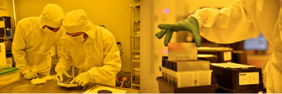
- Level 2: Hands-on Training on Nanofabrication and Characterization Techniques: During ‘Hands on Training’, participants undergo training in the clean room and characterization lab. They learn about the methods and practices of Nanofabrication and Characterization by using equipment in the clean room to make and test basic micro/nano devices. More details: https://www.inup.cense.iisc.ac.in/hands-on-training
- Level 3: Execution of Projects: The very philosophy of INUP is to enable researchers from across the country to carry out their research work without avoidable delays and worries about securing funding for expensive equipment and supplies. Academic researchers without project funding may access the facilities free of cost. After receiving hands-on training, researchers are encouraged to submit their research proposals electronically which are reviewed promptly by domain experts, who work closely with researchers to refine proposals where required. The proposals can be short-term (for a maximum of 3 months) or can be medium-term (from 3 to 24 months). The proposals, which are of duration 2 to 5 years, require collaboration with CeNSE faculty on projects jointly proposed and externally funded. The program also offers similar opportunities to researchers from the industry, on a cost-sharing basis.
Apart from supporting the ‘Research and Innovation Projects’ aimed at academic researchers for executing thesis and research, INUP-i2i shall also support a substantial number of ‘Innovation Projects’ with startup potential. The selection criteria for ‘Research and Innovation Projects’ will continue to be scientific novelty and rigor, whereas the selection criteria for ‘Innovation Projects’ will be translation potential and societal/industrial/strategic relevance. These will be Application-oriented projects - from the Individual Researchers, the Hackathon Winners (comprising GRAND CHALLENGES from different application areas, e.g., strategic, healthcare, agriculture, energy & environment) and the Collaborating Institutes.
B. Mentoring:
- Startup support: This support is for already incubated startups that need micro/nanofabrication and characterization facilities. INUP-i2i will provide continuous technical support for about three years. During this period, technical training, and help in fabrication, optimization, & characterization of devices/systems will be provided.
-
Collaborating Institutes: With the goal of expanding the nanoelectronics/ semiconductor ecosystem in the country, INUP-i2i includes a new model of institute-to-institute engagement along with the six implementing nano centers functioning as hubs connected to a network of Collaborating Institutes. IISc will identify 7 such partners which will comprise institutes from South zone, along with a few from under-served regions of India e.g., the North-East. The engagement will aim for broad and deep R&D collaboration, possibly resulting in joint publications/ patents.
PROGRAM 2:
Indian Nanoelectronics Users Program (INUP) is a program funded by the Ministry of Education, Govt. of India that was initiated in 2019. The program provides basic lecture series training and advanced training (hands-on) to qualified and motivated researchers in the academia at two state-of-the-art facilities, where they may subsequently carry out their research project selected on a competitive basis. Experienced technologists and domain experts assist them, making it possible for aspirants in even remote corners of India to be engaged in very current R&D.
The goals of INUP are: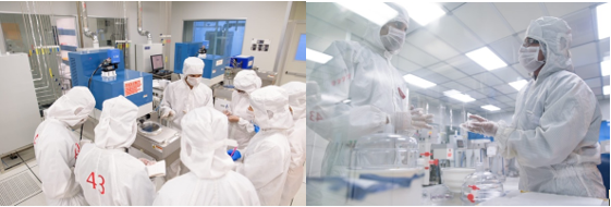
- To promote research in the field of Nanoelectronics
- To provide hands-on-training in Nanoelectronics research to academic investigators from around India
- To provide access to sophisticated facilities for carrying out research projects of current interest
- To provide a platform for researchers to benefit from complementary expertise
- To motivate academics to establish/enhance research programs in their home institutions
For more details, please visit: http://www.inup.cense.iisc.ac.in/