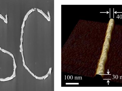
Image: (Left) 'IISc' written in nanoscale using the electrolithography technique developed by the IISc researhers. (Right) The new technique produces lines that are as thin as 40 nanometers.
Image courtesy: Dr Praveen Kumar, IISc
Inside every smart device you use, there are components that used to be bigger just a few years ago. Crucial to the speed and utility of your smartphone or tab is a tiny chip made of different semiconductor materials, onto which tens of thousands of circuits are etched using rather complex methods. A new path-breaking innovation will change how this 'circuit-world' is built.
A team from the Indian Institute of Science has developed a method that could be a game-changer in the semiconductor industry. It will mean faster, cheaper, more efficient patterning of nano-sized circuits at room temperature and ambient conditions; and it does not require chemicals that can harm the environment.
The invention is the result of meticulous studies carried out by Santanu Talukdar, a PhD student jointly supervised by Dr Praveen Kumar and Prof Rudra Pratap. Santanu did most of his research at Centre for Nano Science and Engineering, IISc, one of the best places in the world to carry out nano science research. Also, this is the first technology coming out of India in the high profile area of nanotechnology, and the team believes that this technology has the potential to be in the same league as the top technologies coming from the first world nations.
“The methods used in the industry to write nano-scale circuits require extensive instrumentation to set up and operate. Electrolithography, on the other hand, could even be a table-top setup. Thus, we are not a follower in this area where we generally come up with only incremental changes onto some developed technology; but we are the world wide leader, coming up with a brand new technology and eventually a production tool”, says the team.
The term 'electrolithography' loosely translates into electrically writing on stone (electro + lithos, stone + graphy, to write). In a paper titled “Electrolithography- A new and versatile process for nano patterning” and published in Scientific Reports, Santanu and his advisors have explained this technique: a large electric current passing through pointy electrodes into a thin film of chromium coated on an insulator melts chromium below the negatively biased electrode (cathode) and makes this melt flow away from the cathode. This removes the material only below the cathode, creating a circular trench around it. This is a manifestation of a phenomenon called 'electromigration', which is at the heart of electrolithography: it plays the same role in electrolithography that “hammer and chisel” play in stone carving.
The most major achievement of the semiconductor industry has been to miniaturise, as we all have been observing with the slew of ultrabooks and very thin smart phones. The industry has managed to 'shrink' devices by packing circuits into a tiny area.
A typical microprocessor used in our laptops and phones is as small as a credit card, with billions of electronic components connected to each other. It is inevitable that some of these components are at the nano-scale – a billionth of a metre, or significantly thinner than a human hair. How can you etch circuits at that scale?
“The circuits are written at such a small scale that we need to magnify them tens of thousands of times to make them visible”, the team says. Ironically, it needs big and expensive instruments to achieve that level of miniaturisation. Researchers use ‘electron beam lithography, where the writing is a time consuming serial process. The industry requires a faster and more efficient technique called ‘immersion lithography’. However, ‘Electrolithography’ can potentially revolutionise the manner in which the semi-conductor fabrication industry functions.
The setup involves a thin film of chromium coated on an insulator. When an electric current is passed, the chromium melts and flows away from the negatively biased electrode. The researchers have used tiny electrodes of diameter 10 nanometres, to control the flow of molten chromium, and used it to write the circuits. Something like our pens controlling the flow of ink, but at nano-scale.
By using probes of different diameters, one can draw circuits in varying resolutions: from a few tens of nanometres to a few hundred micrometres. None of the existing semiconductor manufacturing techniques provides this versatility in circuit resolution. Also, unlike the existing methods, this method works well with environmentally friendly chemicals. And, of course, the whole process works under ambient conditions.
While the explorations continue to fine tune the innovation, by using different material electrodes (such as tungsten, carbon nanotube, etc.) and ensuring controlled environments (such as precise control of nitrogen and oxygen); ‘Electrolithography’ may well turn out to be an innovation etched rightly in stone and memory.
Author information:
Santanu Talukdar is a PhD student at the Indian Institute of Science (IISc). He is jointly supervised by Prof Rudra Pratap, Chairman, Centre for Nano Science and Engineering, IISc and Dr Praveen Kumar, Assistant Professor, Department of Materials Engineering, IISc.