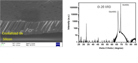
Germanium has significantly high electron and hole mobility compared to silicon, which makes it a promising material for CMOS technology. Ge is used in photonics both as an absorber in near IR as well as a waveguide for mid-IR. Ge is also lattice matched to III-V semiconductors, so good quality III-V films can be grown on Ge substrates. However, integrating device-grade epitaxial germanium on conventional silicon (100) wafers is quite challenging because the lattice parameters of Ge and Si differ by ~4%. This mismatch leads to defects which reduce device performance. In this work we have developed a method to obtain epitaxial germanium on silicon using novel liquid-phase epitaxy method. The resulting Ge films have excellent crystallinity, low dislocation density, and low roughness, making them ideal of a range of applications.
References:
- S. Chaurasia, A. S. Chouhan, S. Raghavan, S. Avasthi, “High-Quality GaAs (100) Thin Films on Silicon (100) Using Epitaxial Germanium (100) Buffer for Low-Cost III-V Solar Cells,” 33rd European Photovoltaic Solar Energy Conference and Exhibition, Amsterdam, September 2017.
- S. Chaurasia, S. Raghavan, S. Avasthi, _High Quality Epitaxial Germanium on Si (100) for low -cost III-V Solar-Cells " 44th IEEE Photovoltaic Specialists Conference, Washington D. C., June 2017
- S. Chaurasia, S. Raghavan, S. Avasthi, Liquid Phase Epitaxy for Growth of High-Quality Crystalline Germanium (100) on Silicon (100) Wafers," 2017 MRS Spring Meeting, Phoenix, AZ, April 2017.