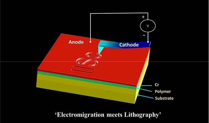
Electrolithography is a new patterning technique developed at CeNSE based on electric field induced material transport. This technique can be used for drawing patterns having dimensions from a few nanometres to a few hundred micrometres at ambient conditions. The uniqueness of this technique is to create etch patterns using electric biased scanning tip as against the conventional patterning techniques based on deep-UV or electron beam irradiation. In the particular case of Cr thin film deposited on an insulating substrate, application of high electric-field between two point electrodes results in liquefaction and subsequent flow of the liquefied material. Electrolithography uses this phenomenon for writing patterns, as described below.
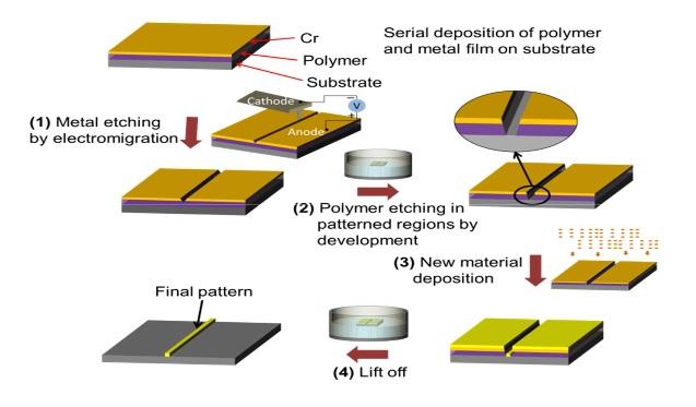
Figure 1:Process flow of the standard electrolithography technique: The process starts with a substrate spin-coated with a polymer followed by the deposition of a top layer of Cr thin film. (1) In the first step, the top Cr layer is etched in the desired pattern using electromigration. (2) Next, the polymer is etched in the patterned region by dipping it in an appropriate solvent. The inset shows the zoomed view of the trench made in the polymer. (3) Subsequently, the desired material is deposited, and (4) lift-off is used to transfer the final pattern on the desired material
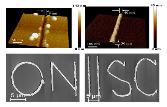
Figure 2: Various patterns created using electrolithography : 3-D AFM images of the narrowest trench in PMMA with a channel width of 9 nm and narrowest Ti thin film line with an average width of 40 nm and thickness 30 nm. Bottom SEM images are of various types of patterns fabricated in Au (75 nm thick) on Si substrate.
Considering the complexity and the cost of the lithography processes, this technique is far better than the e-beam lithography or UV based photolithography, which require high energy e-beam or UV sources, ultra-high vacuum and very expensive instrumentation to reach nano-scale resolutions. To read more about the process please look into http://www.nature.com/articles/srep17753
Patent:
A device, system and method generating structures on a substrate by electromigration, Santanu Talukder, Praveen Kumar, and RudraPratap, Indian patent application -IPA12130001 (filed on 9th December, 2014).