
Research Breakthroughs
 |
Selective killing of cancer-associated fibroblasts by ultrasound-mediated mechanical forcesRead further: https://doi.org/10.1016/j.biomaterials.2025.123844 |
Ultrasound-driven mechanical forces selectively trigger apoptosis in cancer-associated fibroblasts by disrupting key mechanosensory pathways, offering a promising CAF-targeted strategy to enhance cancer therapy.
Read more: DOI: 10.1016/j.biomaterials.2025.123844
To know more, visit:
MEMS Lab led by Prof. Rudra Pratap, CeNSE, IISc.
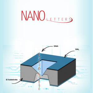 |
Buried Nanopore Membranes with Enhanced Mechanical Robustness for High-Resolution Single-Molecule SensingRead further: https://pubs.acs.org/doi/10.1021/acs.nanolett.5c03778 |
Buried silicon nitride nanopores engineered through a recessed membrane design deliver dramatically improved mechanical durability and high-resolution, label-free DNA sensing—offering a scalable path to robust single-molecule biosensors.
Read more: https://pubs.acs.org/doi/10.1021/acs.nanolett.5c03778
To know more, visit:
Nanopore Research Group, led by Prof. Manoj M Varma, CeNSE, IISc.
 |
Switchable and tuneable high-performance acoustic modes in the L-X band using ferroelectric thin film on sapphireRead further: https://www.nature.com/articles/s41378-025-01080-5 |
BST-based HBARs on sapphire achieve record-high fQ performance with tunable, multi-mode operation—providing a robust, low-power platform for on-chip quantum acoustodynamics, quantum transduction, and quantum information applications.
Read more: https://www.nature.com/articles/s41378-025-01080-5
To know more, visit:
MMNS lab, led by Prof. Gayathri Pillai, CeNSE, IISc.
 |
Disentanglement of physical mechanisms for driving and detection in piezoelectric nanoelectromechanical systemsRead further: https://pubs.aip.org/aip/apl/article/127/14/142202/3366948/Disentanglement-of-physical-mechanisms-for-driving |
- A multimode (Al,Ga)As/GaAs NEMS platform lets researchers clearly separate electrostatic and piezoelectric effects, enabling a fully electrostatic, FET-readout cantilever system and revealing an additional time-delayed drive from chip-wide bulk acoustic waves.
To know more, visit:
NEMS @ CeNSE, led by Prof. Akshay Naik, CeNSE, IISc.
 |
Engineering MoS2–MoTe2 heterojunctions: Enhancing piezoresponse and rectificationRead further: https://pubs.aip.org/aip/jap/article/138/14/144303/3367072 |
Flexible 2D MoS₂–MoTe₂ lateral heterojunctions with asymmetric contacts boost piezoelectric output and rectification, delivering >1 V open-circuit voltages and high power density—offering a promising design pathway for next-gen piezotronic and energy-harvesting devices.
Read more: https://pubs.aip.org/aip/jap/article/138/14/144303/3367072
To know more, visit:
NEMS @ CeNSE, led by Prof. Akshay Naik, CeNSE, IISc.

PEAI-treated SAMs improve perovskite film quality and charge transport, boosting solar-cell efficiency from 19.27% to 21.76% through larger grains, reduced strain, and longer carrier lifetimes.
Read more: https://pubs.acs.org/doi/full/10.1021/acsaem.5c01999
To know more, visit:
Heterojunction Lab, led by Prof. Sushobhan Avasthi, CeNSE, IISc.
 |
Next-Generation Nanopores Enable Real-Time Single-Molecule DetectionRead further: https://doi.org/10.1063/5.0283978 |
Researchers have engineered a versatile nanopore platform that tracks individual molecules with remarkable precision. The study shows how fine molecular interactions can be observed in real time, opening new possibilities for rapid and reliable biosensing and diagnostics. This innovation unites nanofabrication and molecular biology to advance applications from DNA sequencing to drug discovery.
Link to paper: DOI: https://doi.org/10.1063/5.0283978
To know more, visit:
Nanopore Research Group, led by Prof. Manoj M Varma, CeNSE, IISc.

Researchers at CeNSE, IISc, in collaboration with the University of Manchester, have developed a scalable ultramicrotomy-based technique to create atomically precise 2D nanoslit devices from MoS₂. The method enables parallel fabrication of hundreds of identical biosensors capable of detecting single DNA molecules in real time. This fast and cost-effective approach also uncovers unique DNA folding behaviors during translocation, advancing next-generation biosensing and nanofluidic diagnostics.
To know more, visit:
Nanopore Research Group, led by Prof. Manoj M Varma, CeNSE, IISc.
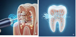 |
Tiny Magnetic Bots Zap Away Tooth Sensitivity PainRead further: https://doi.org/10.1002/advs.202507664 |
Imagine tiny magnetic robots diving deep into your teeth to seal off those pesky exposed nerves causing sharp pain from cold drinks or air—now, that’s no sci-fi dream! Researchers at CeNSE have engineered “CalBots,” smart nanomaterials that self-assemble under magnets to plug dentinal tubules over 300 microns deep, offering lasting relief where toothpastes fall short. Dive into this breakthrough to see how it could transform dentistry and end the wince for billions worldwide.
Magnetic Bioceramic Nanoparticles Enable Deep Tubule Sealing for Long-Term Dental Hypersensitivity Relief
Link to paper: https://doi.org/10.1002/advs.202507664
To know more, visit:
Quant2m, led by Prof. Ambarish Ghosh, CeNSE, IISc.
 |
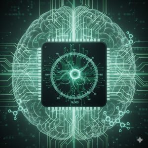
Brain-Like Blueprints: Redesigning AI Hardware for a Smarter, Greener FutureRead further: : https://www.nature.com/articles/s41928-025-01432-z |
Imagine AI chips that think like the human brain, slashing massive energy use while powering lightning-fast, privacy-secure devices right at your fingertips. CeNSE innovators expose the hidden pitfalls in today’s neuromorphic tech—like noise buildup and wire glitches—and chart disruptive new paths to overcome them, promising a revolution in sustainable computing. Dive in to see how this could make AI not just powerful, but planet-friendly too!
Link to paper: https://www.nature.com/articles/s41928-025-01432-z
To know more, visit:
MoNC-AI, led by Prof. Sreetosh Goswami, CeNSE, IISc.
 |
Tiny Sound Machines: Crafting Tunable Frequency Combs for Smarter Sensors and BeyondRead further: https://pubs.aip.org/aip/jap/article/138/10/104502/3363261/Tunable-phononic-frequency-combs-in-curved |
Picture microscopic ultrasound devices that dance with sound waves, creating customizable “combs” of frequencies through clever mode interactions—like tuning a radio to unlock new signals! CeNSE scientists have harnessed nonlinear resonances and special ferroelectric films in curved transducers to generate these adjustable combs, revolutionizing how we manipulate mechanical vibrations. Explore this sonic breakthrough to see its potential in super-sensitive detectors, acoustic imaging, and even phonon-powered computing.
link to paper: https://www.nature.com/articles/s41598-025-00617-y
https://pubs.aip.org/aip/jap/article/138/10/104502/3363261/Tunable-phononic-frequency-combs-in-curved
To know more, visit:
MMNS lab, led by Prof. Gayathri Pillai, CeNSE, IISc.
 |
Molecular Magic Unlocks Perfect Brain-Like Switches for Smarter AIRead further: https://doi.org/10.1063/5.0256247 |
Imagine computers that learn like human brains, but without the messy glitches—CeNSE scientists have engineered a tiny molecular switch that flips states with flawless linearity and symmetry over 16,500 levels, turning nonlinear chaos into precise control. This breakthrough harnesses everyday molecules to supercharge neuromorphic hardware, slashing energy use and boosting AI performance. Peek inside to see how it could redefine computing and spark the next tech revolution.
Kinetically Tuned Molecular Mechanism Achieves Near-Ideal Linearity and Symmetry in Neuromorphic Elements for Advanced Computing
Link to paper: https://doi.org/10.1063/5.0256247
To know more, visit:
MoNC-AI, led by Prof. Sreetosh Goswami, CeNSE, IISc.
 |
Where is the electricity flowing?Read further: JPCM, https://iopscience.iop.org/article/10.1088/1361-648X/ade7e6 |
Multichannel conduction in electron transport dynamics of three dimensional topological insulators
In this study on BiSbTeSe₂ (BSTS), researchers uncovered smarter ways to distinguish surface and bulk contributions to electrical flow using magnetic fields and nonlinear Hall effect measurements. This work brings us closer to designing next-gen electronic devices built on these remarkable materials!
Read More: JPCM, https://iopscience.iop.org/article/10.1088/1361-648X/ade7e6
Learn more about how Dr. Dhavala’s group is working on unlocking the potential of topological insulators for future technologies. https://sites.google.com/view/qmatinlab/home
 |
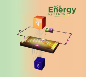
What if gas sensors didn’t need power?Read further: Small 2025, 2503284. https://onlinelibrary.wiley.com/doi/10.1002/smll.202503284 |
Can One Material Detect Two Gases at Once—Without Power?
A collaborative research between CeNSE, IISc, IIT Kharagpur and IISER Trivandrum has resulted in a new study that explores MoO₂–MoSe₂ heterostructures created in a single-step CVD process for self-powered gas sensing at room temperature.
Key Highlights:
- S1 (MoO₂-rich) selectively detects H₂
- S2 (MoO₂–MoSe₂ heterostructure) shows high NO₂ sensitivity down to 10 ppm, enhanced by visible light and humidity
- No external power required
- Two flake types = complementary sensing
- Potential: Wearables, aerospace, and smart sensing arrays
Read More: Small 2025, 2503284. https://onlinelibrary.wiley.com/doi/10.1002/smll.202503284
Lear more about the Research work conducted by Prof. Navakanata Bhat’s work here: https://www.cense.iisc.ac.in/navakanta-bhat/
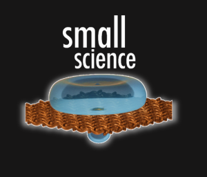 |
What Happens when a droplet hits a sieve?Read further: Small Sci. 2400586. (2025), https://onlinelibrary.wiley.com/doi/10.1002/smsc.202400586 |
Researchers from Microfluidic Devices & Heterogeneous Systems Lab have discovered a novel recoil cavity mechanism that enables precise single-droplet generation during liquid impact on superhydrophobic sieves. Unlike traditional methods, this unique two-stage process involves the formation of a secondary recoil cavity, triggered by the collapse of the initial impact cavity — a phenomenon never observed on other surfaces!
The study offers new insights into cavity dynamics and paves the way for highly controlled droplet-based printing, with exciting applications in electronics, biology, and structural fabrication.
Read the full paper: Small Sci. 2400586. (2025), https://onlinelibrary.wiley.com/doi/10.1002/smsc.202400586
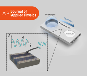 |
What secrets lie beneath suspended graphene?Read further: Appl. Phys. 137, 215302 (2025): https://doi.org/10.1063/5.0268038 |
New insights into graphene–liquid interactions!
A recent study explores how suspended graphene membranes behave at the polar liquid–air interface within a microfluidic platform.
Using dynamic atomic force microscopy, researchers uncovered how graphene:
— Eliminates capillary instabilities at the liquid interface
— Enables stable, high-resolution phase imaging of defects like micro/nanoholes
— Seals the channel even with imperfections, thanks to trapped nanoconfined water
— Creates a powerful platform for biosensing and nanomechanical applications
This work strengthens the foundation for graphene-integrated microfluidic devices and offers new avenues for studying confined water physics.
🔗 Read the full publication at: J. Appl. Phys. 137, 215302 (2025): https://doi.org/10.1063/5.0268038
Read about the research work from Prof. Akshay Naik’s group: https://www.cense.iisc.ac.in/akshay-naik/
 |
Unlocking Carrier Mobility in PerovskitesRead further: ACS Energy Lett. 2025, 10, XXX, 3074–3080, https://pubs.acs.org/doi/10.1021/acsenergylett.5c01151 |
Measuring charge carrier mobility in resistive perovskites has long posed a challenge. Researchers at CeNSE, IISc have now developed a reliable, low-noise photo-Hall measurement technique that accurately extracts electron and hole mobilities—even at ultra-low light intensities.
Their study shows that methylammonium lead iodide (MAPI) can exhibit n-type behavior in the dark and p-type under light—a surprising result driven by unequal charge mobilities. This insight helps resolve long-standing inconsistencies in reported mobility values and enhances our ability to characterize materials for solar cells and optoelectronics.
Read the full paper here: ACS Energy Lett. 2025, 10, XXX, 3074–3080, https://pubs.acs.org/doi/10.1021/acsenergylett.5c01151
Read about the research work from Prof. Sushobhan’s group here:
 |
Energy-efficient, high-performance neuromorphic hardwareRead further: ACS Energy Letters 2025 10 (5), 2193-2202, https://pubs.acs.org/doi/10.1021/acsenergylett.5c00411 |
A collaborative effort between CeNSE, IISc, and IIT Kanpur results in the development of lead-free Cs₃Bi₂I₉ perovskite memristors that mimic brain-like synapses—bringing us closer to next-gen, low-power neuromorphic computing.
This work marks a key advancement in lead-free, low-dimensional halide perovskites for neuromorphic hardware. It addresses critical issues like variability, nonlinearity, and sneak-path currents in memristor arrays, enabling reliable, high-yield performance. The materials are environmentally safe and suitable for scalable, flexible AI edge devices. With stable switching and uniformity, this research supports energy-efficient, real-time processing, paving the way for practical, neuromorphic systems in wearable electronics and edge-based AI applications.
Read more: ACS Energy Letters 2025 10 (5), 2193-2202, https://pubs.acs.org/doi/10.1021/acsenergylett.5c00411
Read more about the research work from Dr. Aditya Sadhanala’s group here: https://www.cense.iisc.ac.in/aditya-sadhanala/
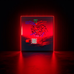 |
Brightening the Future of DisplaysRead further: Nanoscale 2025, 17, 7753, https://pubs.rsc.org/en/content/articlelanding/2025/nr/d4nr05253f |
FRET-Driven Ultra-Vivid Pure-Red Emission Breakthrough in Polymer-Perovskite Hybrid Matrices
Integrating Perovskite nanocrystals (PeNCs) into polymer matrices unlocks an exciting pathway to dramatically enhance perovskite emission properties. By harnessing the power of Förster Resonance Energy Transfer (FRET) in polymer–PeNC composites, we achieve extraordinary improvements in photoluminescence efficiency, resulting in vibrant, ultra-pure red emission.
This breakthrough highlights the immense potential of polymer–PeNC blends to deliver highly efficient, vivid red-emitting materials, paving the way for next-generation displays and advanced optoelectronic applications.
 |
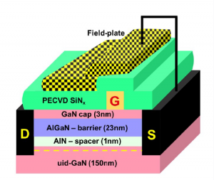
Breakthrough in Compensation free HEMT on Si for X Band Power PerformanceRead further: Phys. Status Solidi RRL, 2025, 2400409 at https://doi.org/10.1002/pssr.202400409 |
Successful demonstration of the microwave power performance of AlGaN/GaN HEMTs on silicon at X-band frequencies. Notably, this achievement was realized using a polarization-graded buffer without any compensation doping, such as iron or carbon, in the stack. At the 2 dB compression point, the devices delivered 8 W of output power at 10 GHz with a drain efficiency of 46%. Further improvements are anticipated with substrate thinning and enhanced thermal management.
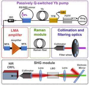 |
Tunable multi-color fiber laser source and applications in photoacoustic imagingRead this article published in Optics letters, Vol. 50., Issue. 7, pp 2223-2226 (2025) at https://doi.org/10.1364/OL.553618 |
A novel tunable multi-color pulsed laser system as a compact, cost-effective alternative to supercontinuum and optical parametric oscillator (OPO) sources for biomedical imaging. Emitting in both the near-infrared (1060–1600 nm) and visible (530–600 nm) regions, it enables advanced applications like photoacoustic imaging (PAI). We demonstrate photoacoustic spectroscopy of lipids, a capability previously achievable only with OPOs, expanding the potential for biomedical research.
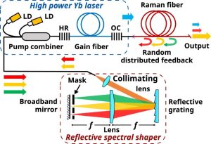 |
Enhanced linewidth control in wavelength agile Raman fiber lasers using Fourier spectral shapingRead further: Optics Letters, Vol. 50, Issue 1, pp 201-204 (2025) at https://doi.org/10.1364/OL.544060 |
Cascaded Raman fiber lasers (CRFLs) can produce light at various wavelengths in the near-infrared (NIR) region, but their output is usually spectrally broad. In this work, researchers have introduced a new feedback method using Fourier spectral shaper that provides tunable filtered feedback, which helps narrow the output spectrum by about three times. This improvement is achieved without affecting the laser’s ability to tune across different wavelengths, while still delivering high power in the multi-watt range.
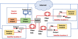 |
Remote Characterization and Dissemination of Dispersion Compensated Ultrashort Pulses Through Dynamic Fiber Optic LinksRead further in IEEE, photonics journal at https://doi.org/10.1109/JPHOT.2025.3529627 |
Ultrafast Lasers are complex pieces of equipment. It is desirable to have one source serve multiple locations and experiments for cost reduction. This can be accomplished through the dissemination of pulses to satellite locations through fiber optic links. However, the fidelity of pulses received and compensating dispersion effects requires thorough characterization. Requiring complex characterization equipment at all satellite location undoes the gains. In the work presented here, we overcome this problem.
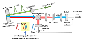 |
Remote characterization of nonlinear distortions in ultrashort pulses transmitted through dynamic fiber optic linksRead this article published in Optics Express, Vol. 33, Issue 2, pp. 2158-2168 at https://doi.org/10.1364/OE.545372 |
Here, we have introduced a method for remotely detecting the optical nonlinearities seen by ultrashort pulses in the fiber link. By integrating a custom-fabricated fixed delay interferometer with a quartz plate with partially reflecting Bragg mirrors to the detector module, we can accurately capture nonlinear distortions in sub-400 fs pulses. The detector module uses simple optics with non-movable parts and minimal footage, easily replicable at multiple target locations to facilitate pulse measurements. Thus, with robust delivery and characterization of both dispersive and nonlinear effects, this approach can significantly increase the efficacy of ultrafast laser sources and reduce overheads.
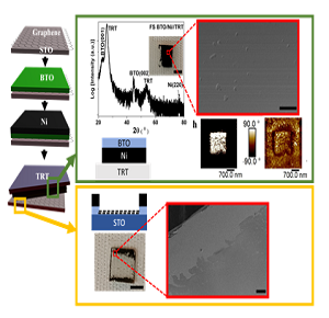 |
Free Standing epitaxial oxides through remote epitaxyRead this article published in Nanoscale 17, 2025, pp. 2020-2031 at https://doi.org/10.1039/D4NR03356F |
Epitaxial BaTiO3 (BTO) was grown via remote epitaxy using CVD graphene, and freestanding membranes were subsequently transferred onto Si. We identified a correlation between the graphene microstructure, its defect formation under pulsed laser deposition, and the crystalline quality of the deposited BTO film.
 |
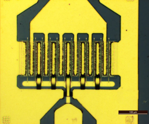
High-Performance Graphene-Based Pressure SensorClick to read further: https://iopscience.iop.org/article/10.1088/ 1361-6439/ad5561 |
Researchers from the NEMS@CeNSE laboratory have created a highly sensitive graphene-based pressure sensor. It works by measuring changes in resonance frequency when pressure deforms a thin silicon diaphragm. This sensor is much more responsive than traditional silicon sensors, with a record-high performance of 20 kHz/kPa and potential up to 500 kHz/kPa. It can detect very small pressure changes (as low as 90 Pa). The design is simple, adaptable, and could be integrated into modern semiconductor manufacturing, making it highly practical. Read the complete article here at: More, S., & Naik, A. (2024). Graphene resonant pressure sensor with ultrahigh responsivity-range product. Journal of Micromechanics and Microengineering, 34(7), 075006.
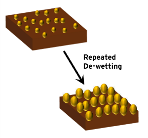 |
Enhanced Sensitivity in SERS Detection Using De-wetted Metal SubstratesClick to read further: https://doi.org/10.1016/j.apsusc.2024.161096 |
Surface-enhanced Raman spectroscopy (SERS) enhances molecular detection on metal surfaces or nanostructures. This study highlights that repeated de-wetting of metal thin films boosts SERS sensitivity over tenfold by creating closely spaced metal nanoclusters that amplify electromagnetic fields. The substrates detect Rhodamine 6G at sub-femtomolar levels and amino acids at micromolar levels. These findings suggest potential for integrating these substrates with nanopores for effective SERS-based sensing at confined, high-concentration conditions. Read the complete article here at: Pal, A., Roshini, R. A., & Varma, M. M. (2024). De-wetted gold nanostructures for SERS-based sensing of static and dynamic targets. Applied Surface Science, 678, 161096.
 |
Enhanced Analysis Method for Energy Loss in Piezoelectric MEMS DevicesClick to read further: https://ieeexplore.ieee.org/abstract/ document/10705914 |
This research presents a new method using synchronized optical and electrical measurements to better analyze and improve piezo-MEMS devices. Piezoelectric microelectromechanical systems (MEMS) have great market potential due to their efficient energy conversion. However, energy loss in piezoelectric films can reduce device performance. Current methods to measure energy loss are not ideal for thin-film devices where energy storage and dissipation are spread across layers. The method is demonstrated using specialized MEMS components, enhancing accuracy and performance insights. Read the complete article here: Kumar, V., Tiwari, S., Pillai, G., Pratap, R., & Chandorkar, S. A. (2024). Synchronized Opto-Electro-Mechanical Measurements for Estimation of Energy Dissipation in Thin-Film-Piezoelectric-on-Substrate MEMS/NEMS Devices. Journal of Microelectromechanical Systems.
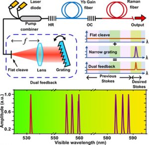 |
Want to reduce the linewidth of Raman fiber lasers?Click to read further: https://opg.optica.org/oe/fulltext.cfm?uri=oe-32-12-20629&id=551029 |
Use dual feedback! Then frequency double it to get >100 mW single mode power in visible.
Raman lasers can generate power at any wavelength, but the output spectrum is very broad. Researchers at CeNSE have found that by using the proposed “dual feedback” mechanism, linewidth reduction of ~ 5x is achieved at any wavelength. Frequency doubling this linewidth-reduced near infrared source, >100 mW single mode light of ~ 0.05 nm linewidth in green to yellow is generated.
This paper was published in Optics Express, Vol. 32, No.12, 3 June 2024.
 |
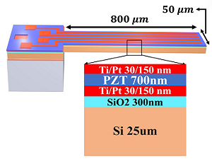
Waveguides for use in programmable photonic integrated circuits and neural network platformsClick to read further: https://pubs.aip.org/aip/apl/article-abstract/124/23/231105/3296495/Silicon-loaded-waveguide-in-sputter-deposited-PZT?redirectedFrom=fulltext |
In this work, researchers developed an architecture that uses silicon-loaded PZT as the waveguide to realize a modulator to help overcome the electro-optic interaction issue faced in conventional architecture. The device enhanced EO response by 400% is attributed to the improved electro-optic overlap as well as PZT film quality.
The article was published in Applied physics Letters, AIP Publishing, 124, 231105, (2204).
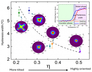 |
EPITAXIAL INTEGRATION OF VO2 ON TO SILICON UNVEILS TEXTURAL CONTROL OF HYSTERESISCheck out more details on this article at: https://www.sciencedirect.com/science/article/pii/ S2589152924000826?via%3Dihub |
Vanadium Dioxide (VO₂) exhibits a fascinating metal-insulator transition (MIT) used in various applications. However, tailoring its phase transition hysteresis is crucial, for example sensors require minimal hysteresis while memories need a larger value.
In this study, researchers address two problems:
(a) epitaxial integration of VO2 onto Si(100), &
(b) use this as a model system to study the correlation between texture and phase-transition hysteresis in VO2 thin films.
The paper was published in Elsevier, Materialia, Vol. 34, May 2024, 102085.
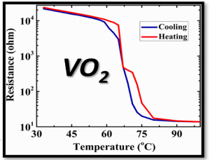 |
VO2 neuristors show large electro optic mechanical effectsCheck out more details on this article at: https://pubs.aip.org/aip/apr/article-abstract/11/2/021410/3283130/Large-electro-opto-mechanical-coupling-in-VO2?redirectedFrom=fulltext |
Researchers from CeNSE and SSCU, IISc demonstrated that VO2 based neuristors, produced electro-mechanical self-oscillatory behavior akin to biological neurons. High piezoelectric and electrooptic coefficients make it a promising candidate for diverse applications necessitating efficient energy conversion and optical modulation.
The research was published in AIP Publishing, Appl. Phys. Rev. 11, 021410 (2024).
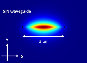 |
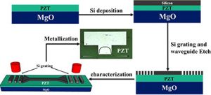
Shaping the Future: Embedded Si Gratings Enhance Thin Film SiN WaveguidesClick to read further: https://doi.org/10.1364/OE.488999 |
Researchers from the Photonics Research laboratory have developed an innovative silicon embedded grating coupler to improve fibre-chip coupling. The demonstration has far-reaching implications in quantum photonic integrated circuits, on-chip sensors, LiDAR and RADAR applications.
 |
Unlocking Neuron-Like Self-Oscillations: Paving the Way for Low-Power Neuromorphic HardwareClick to read further: https://doi.org/10.1021/acsaelm.3c00549 |
The all-or-nothing law ensures the nerve cell fires at full strength or doesn’t. Members of the microsystems & fluctuations dissipation lab have demonstrated neuron like self-oscillations in thin films of NdNiO3.
 |
Mastering Impact Dynamics: How Particle-Coated Droplets Take Control of Pinch-Off PhenomenaClick further: https://doi.org/10.1016/j.jcis.2023.05.067 |
Research conducted by the Microfluidic Devices & Heterogeneous Systems lab has revealed critical insights into the factors that govern the stability of droplets during impact. This knowledge has significant implications for various applications, including printing, spraying, pesticide delivery, and cooling processes.
 |
Breaking Barriers: Setting Record Mobility Values in Semiconductor InnovationClick to read more: https://doi.org/10.1039/D3TC00789H |
Researchers from the Heterojunction lab have systematically investigated the controlled growth of Cu2O using CVD and demonstrated record values of hole mobility and field-effect mobility. These CVD-deposited films are repeatable, scalable and relevant for transistors, displays drivers, and sensors.
 |
BEYOND PROTECTION: MOBILE SCREEN PROTECTORS AS SUBSTRATES FOR NEXT-GEN PIEZOTRONIC DEVICESClick to read more: https://ieeexplore.ieee.org/document/9998109 |
Piezotronics are the new-age semiconductor devices that find applications in sensors, flexible electronics and nanorobotics. Researchers at the NEMS@CeNSE lab have used these inexpensive, readily available, easily peelable flex screen protectors to fabricate 2D material devices.
 |
BOOSTING POWER AND EFFICIENCY: ENHANCING THE PERFORMANCE OF GAN HIGH ELECTRON MOBILITY TRANSISTORSClick to read more: https://ieeexplore.ieee.org/document/10049388 |
GaN HEMTs are crucial for high-power Radio Frequency (RF) applications like next-generation wireless communication and radars. Researchers from the Semiconductor Devices Lab have fabricated transistors on such a polarization-engineered platform displaying excellent dynamic performance, approaching state-of-the-art for GaN HEMTs on Silicon.