We do comprehensive modelling, simulation and experimental work on devices to develop the appropriate device structure, gate dielectric, junctions etc. Some recent highlights include ideal-Schottky contact development on Germanium, a novel transistor structure – HFinFET – for III-V, demonstration of very high ON to OFF current ratio on Graphene transistors.
Layered 2D semiconductors, particularly of the MX2 family, are attracting a lot of attention among the device community for their unique material and electron transport properties that can enable next-generation electronics. At CeNSE, we do large-area CVD growth of such materials and enable various device topologies including integration with other semiconductors. Besides, the optical properties of 2D materials are of interest in novel photodetection and manipulation. For example, the plasmonic-Graphene sandwich structures recently developed at CeNSE gave rise to record sensitivity in the visible region (see photonics page for more details).
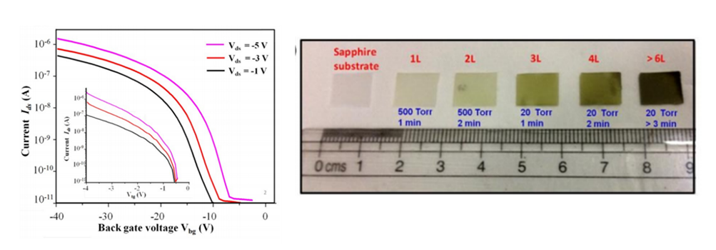
Figures: (left) I-V characteristics of back-gated MoS2 FET. (Right): Image showing MoS2 of various layers grown on sapphire indicating excellent control on number of layers.
 Professor |