Nanotechnology is all about scaling down the size of devices. The logical extreme of this effort are low-dimensional semiconductors whose critical dimension is only one or few atoms thick. 1D semiconductors like carbon nanotube and 2D semiconductors like graphene, belong to this class of materials. CeNSE has a very successful program to deposit these exciting materials over large areas for various applications.
At the core of the research is an in-house designed and constructed chemical vapor deposition system with a very low oxygen partial pressure of 10-25 Torr. The reactor is especially suited to deposit very high-quality low-dimensional materials, such as Si nanowires, graphene, WSe2, MoS2 & BN. In keeping with the collaborative tradition, the reactor is used by several research groups, within and outside IISc, to grow 1-D and 2-D materials for applications ranging from high-performance flexible electronics, packaging, suspended MEMS devices, and beyond-CMOS devices.
1. 1D materials -- Si Nanowires
Nanowires are high-aspect ratio materials where the length of the “wire” is up to 1000x larger than the diameter. Nanowire “forests” of the type shown below have a very large surface area to volume ratio, making them very useful for supercapacitors, purifying membranes, transparent electrodes, etc. Nanowires can also be very anisotropic with different properties along and orthogonal to the wire length. The anisotropy can be leveraged in next-generation solar cells and transistors. Finally, nanowires have been shown to have excellent mechanical properties, with applications in various types of coatings.
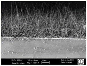
A Silicon nanowire forest
Representative Publications
i) D. Shakthivel, S. Raghavan, “Vapor-liquid-solid growth of Si nanowires: A kinetic analysis”, Journal of Applied Physics 112, 024317 (2012); doi: http://dx.doi.org/10.1063/1.4737597
2. 2D Materials – Graphene, MoS2, WSe2, & BN
CeNSE works on a whole library of 2D materials, such as graphene which is a conductor, MoS2 & WSe2 which are both semiconductors, and BN which is an insulator. These materials provide the ultimate in device scaling because they limit the current to a layer that is just 1 atom thick. With the Si CMOS rapidly reaching the limit of scaling, 2D materials are promising candidates next-generation electronics devices.
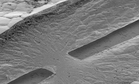
A suspended graphene layer that is only one atom thick!
Representative Publications
i) K. Roy, M. Padmanabhan, S. Goswami, T.P. Sai, G. Ramalingam, S. Raghavan, A. Ghosh, “Graphene-MoS2 hybrid structures for multifunctional photoresponsive memory devices, “ Nature nanotechnology 8 (11), 826-830
ii) A. Nath Pal, S. Ghatak, V Kochat, E. S. Sneha, A. Sampathkumar, S. Raghavan, and A. Ghosh, “Microscopic Mechanism of 1/f Noise in Graphene: Role of Energy Band Dispersion,” ACS nano 5 (3), 2075-2081 (2011).
iii) V. Kochat, A. N. Pal, S. Ghatak, E. S. Sneha, A. Sampathkumar, A. Gairola, S. A. Shivashankar, S. Raghavan, and A. Ghosh, “High contrast imaging and thickness determination of graphene with in-column secondary electron microscopy,” J. Appl. Phys., 110, 014315 (2011).
iv) V.K. Kumar, S. Dhar, T.H. Choudhury, S.A. Shivashankar, S. Raghavan, “A predictive approach to CVD of crystalline layers of TMDs: the case of MoS2,” Nanoscale 7 (17), 7802-7810
v) S. Kumar, G.S. Duesberg, R. Pratap, S Raghavan, “Graphene field emission devices,” Applied Physics Letters 105 (10), 103107S. (2014)
vi) S. Kumar, S. Kaushik, R. Pratap, S. Raghavan, “Graphene on paper: A simple, low-cost chemical sensing platform,” ACS applied materials & interfaces 7 (4), 2189-2194 (2015)
vii) P.K. Basu, D. Indukuri, S. Keshavan, V. Navratna, S.R.K. Vanjari, S. Raghavan, N. Bhat, “Graphene based E. coli sensor on flexible acetate sheet,” Sensors and Actuators B: Chemical 190, 342-347 (2014)
viii) P. Ghosh, S. Kumar, G. Ramalingam, V. Kochat, M. Radhakrishnan, S. Dhar, S. Suwas, A. Ghosh, N. Ravishankar, S. Raghavan, “rinivasan Raghavan, “Insights on defect-mediated heterogeneous nucleation of graphene on copper,” The Journal of Physical Chemistry C 119 (5), 2513-2522.
 Associate Professor |
 Professor |