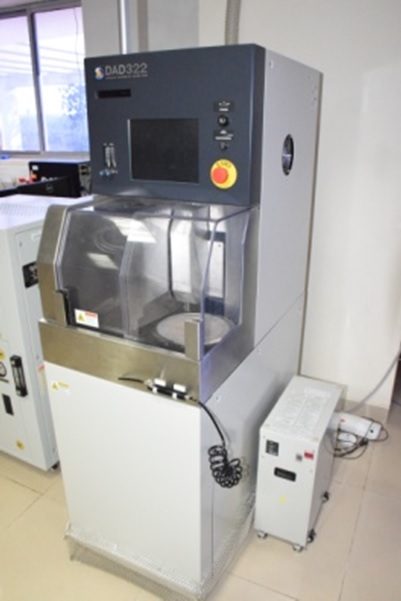
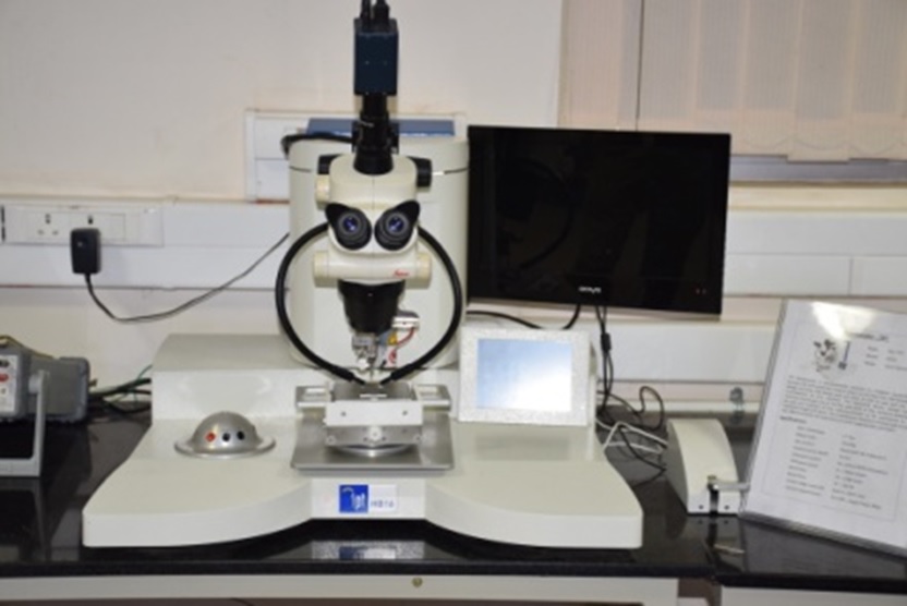
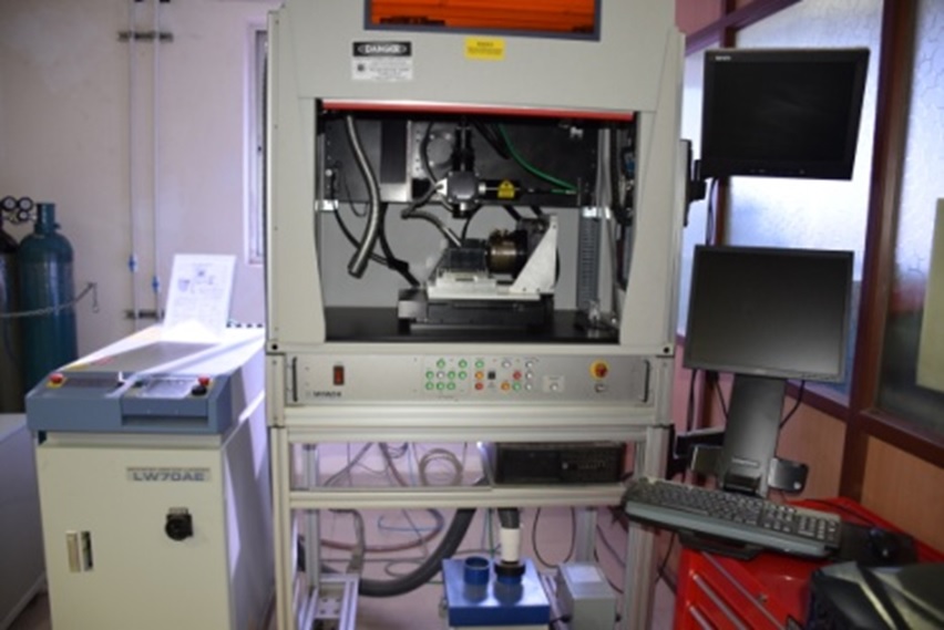
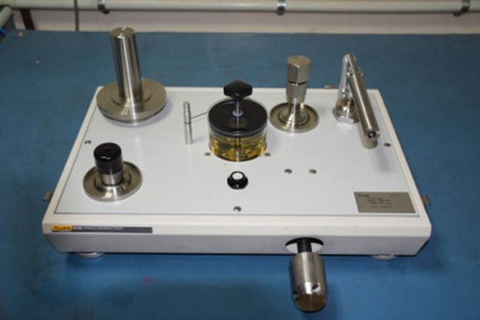
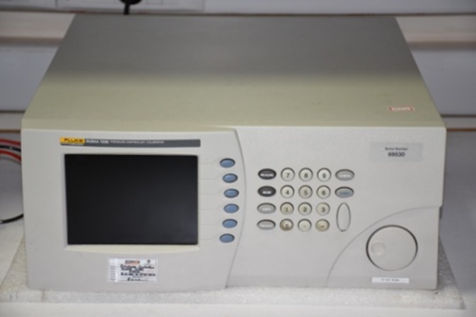
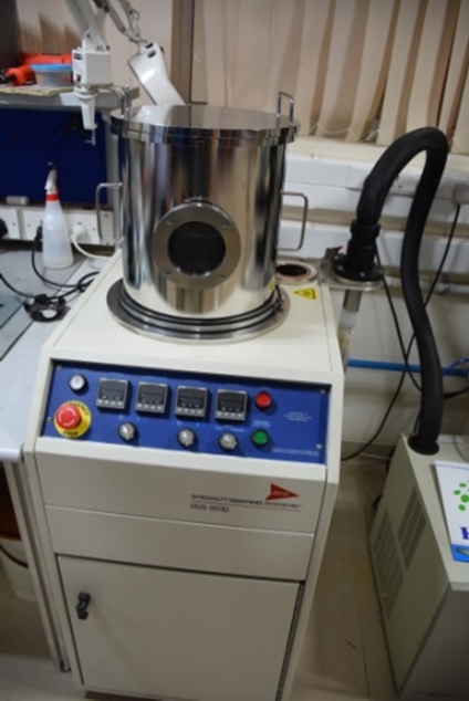
Located in the third floor of the CeNSE building #TF 32 is a 2000 sq feet lab, housing most of the infrastructure to enable packaging of various MEMS devices. The lab has facilities for Wafer Dicing, Die Attach, Ball/Wedge bonding, Laser welding, Soldering, Visual Inspection Microscope, Oil filling station as well as for Assembly-and-package-level testing of MEMS devices. It also has facilities for Low / High level pressure calibration, Acoustic calibration and data acquisition systems for performance studies and characterization of various transducers. As one of the supporting the central facilities available at CeNSE, the MEMS and IC Packaging lab provides all the facilities required to build a packaged device using a wafer. Following equipments housed in MEMS packaging lab are available to user's with appropriate permissions.