Layered 2D materials offer great promise in extending Moore’s law due to their excellent electrostatic control and atomically thin nature. 2D materials of the transition metal dichalcogenide (TMD) family, such as MoS2, WSe2 , etc., are of particular interest for transistor applications. However, there are significant challenges posed by these materials, ranging from poor contact, high-k dielectric integration to efficient p-doping. Here at CeNSE, we develop processes to mitigate these challenges and design transistors of excellent performance.
We have developed processes such as sulfur treatment for contact engineering on MoS2 and integrated it with high-k HfO2 dielectric for high-performance Field-Effect Transistors (FETs). We have also demonstrated a sub-thermionic transistor that surpasses the Boltzmann limit of 60 mV/dec sub-threshold slope. Recent research includes developing processes for channel-length scaling, p-type FETs, CMOS logic integration, etc.
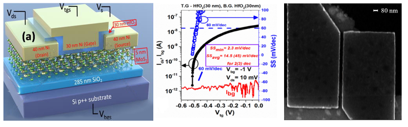
Figure: (left) Sub-thermionic FET using MoS2 and its transfer characteristics, (middle) & (right) SEM image of a short-channel FET using MoS2 with a gate length of 80 nm
 Professor |
 Professor |