Gallium Nitride (GaN) transistors for power and RF applications:
Due to unique material properties such as high polarization, wide band gap, high carrier mobility and velocity, Gallium Nitride and its alloys (III-nitride family) have enabled transistors with much superior performance compared to traditional silicon devices in the areas of high-power switching and RF power amplification.
In the area of high-power switching, GaN transistors are entering the market primarily in the 600 V segment and are usually enabled on silicon substrate for cost and scalability reasons. However, this presents enormous material challenges in terms of high dislocation density, defects, wafer bow and stresses which directly affect device performance. Additionally, to reduce the spurious background charge, carbon is added intentionally to reduce leakage and enhance breakdown voltages, but this degrades the ON state of the transistors. At CeNSE, materials scientists and device engineers work in sync to study the correlation between material and microstructural qualities of GaN-on-silicon vis-a-vis device operation and performance. The interplay of carbon doping, dislocation, breakdown voltage and dynamic ON resistance is studied, while dielectrics, interfaces and traps are also carefully investigated. In parallel, there is an active effort directed toward developing large-periphery transistors for realizing 30 A, 600 V devices under the technology development umbrella. Process development, understanding the various unit processes and design of such wide periphery devices are being undertaken.
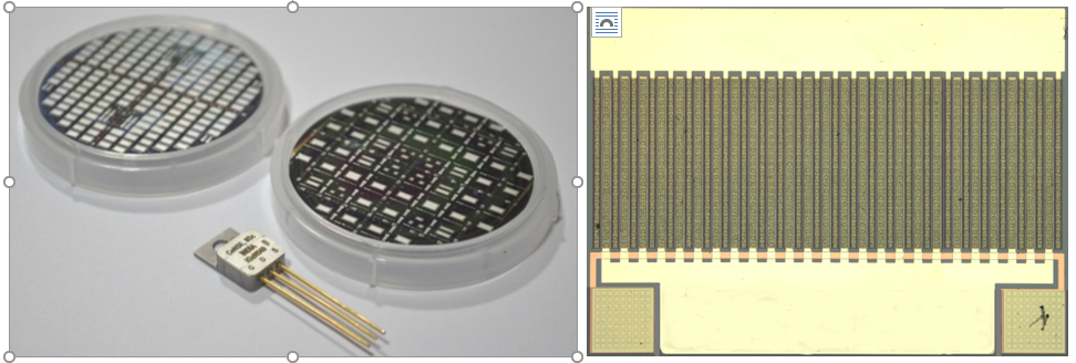
Figure 1: (left) fully fabricated 5 A, 40 V GaN transistors (including packaged device) on an indigenously developed material platform, (right) Optical micrographs of 50 mm wide large-periphery GaN HEMTs for high-power switching applications.
In the area of RF devices, GaN transistors are being explored primarily on silicon substrate, targeting applications ranging from C-band to mm-wave. We are working on making deep sub-micron devices for very high cut-off frequencies, passivation schemes for reducing current collapse, Au-free Ohmic contact schemes and novel metal stacks for reduced contact resistance and surface roughness.

Figure 2: (left) SEM image of a deep sub-micron GaN transistor with cut-off in the mm-wave, (right) output characteristics of deeply scaled transistor, showing high current densities.
Ultrawide band gap semiconductor-based deep-UV detectors:
Deep-UV detectors operating in the UV-B (325-290 nm) and solar-blind regime (290 nm and below) are of strategic importance besides being promising candidates for UV astronomy, ozone monitoring, wearable sensors to monitor sun burn, and many more.
At CeNSE, we work with aluminium gallium nitride (AlGaN) – a GaN-based alloy, as well as with emerging gallium oxide (Ga2O3) to develop deep-UV detectors with excellent performance. Growth of epitaxial AlGaN alloy on sapphire and on silicon, with alloy composition ranging from 0 to 60%, have been extensively investigated, and state-of-the-art detectors in planar MSM as well as in vertical p-i-n geometries have been developed. We work on correlating the defect-microstructure and device performance of these photodetectors while demonstrating record-high responsivity and some of the highest device parameters like UV to visible rejection ratio and photo-to-dark current in the world.
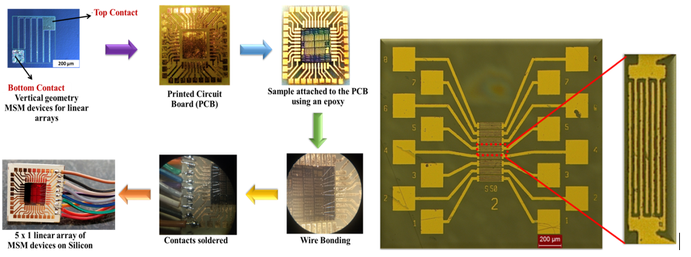
Figure 3: (left) a single p-i-n detector based on AlGaN which is then bonded to a PCB, and arrays of such devices are demonstrated toward possible focal plane array development, (right) Linear array of UV detectors based on bulk Ga2O3 crystal (collaborators: IGCAR, Kalpakkam).
We are working on developing an in-house mist CVD platform, with which we can grow stable phase of α-Ga2O3 and demonstrate deep-UV photodetectors based on this material. In collaboration with national and international peers, we have also shown state-of-the-art performance in epitaxial β-Ga2O3 detectors. Our current focus is on the study of optical properties of ε-phase of α-Ga2O3 vis-a-vis its structural properties.
 Associate Professor |
 Professor |
 Visiting Professor |