Sorry, you need to enable JavaScript to visit this website.
office.cense@iisc.ac.in | +91-80-2293 3276/ +91-80-2293 3291 | Sitemap

The centre offers MTech and PhD degree programs in the area of nano science and engineering.
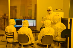
Clean room 1 (2)M. Engg. in Semiconductor Technology:
CeNSE is launching a one-year M.Engg in Semiconductor Technology from the Academic year 2024-25 (Aug'24). The objective is to align with the India Semiconductor Mission to cater to the fast-growing semiconductor ecosystem in the country in particular and in the world in general. The semiconductor industry is vast and has its requirements not just from the core subjects but from a vast range of fields. This program is designed be attractive to students from multiple streams & backgrounds while at the same time aligning with the current industrial relevance of semiconductor technology vis-a-vis the demand for skilled workforce and cutting-edge R&D in semiconductor technology.
Along with guidance from experts in the field, the selected students benefit from Industrial interactions at CeNSE, CeNSE and cutting-edge R&D facilities.
Selection: 70% based on GATE score & CGPA >=8.0 (for students from CFTIs) + 30% based on interview
Duration: One year
Eligibility: BE / B Tech or equivalent degree in any discipline or M Sc or equivalent degree in electronics engineering, electrical engineering, mechanical engineering, materials engineering, chemical engineering, instrumentation engineering, physics, applied physics, photonics, material science, chemistry, etc.
Approximately 20 students will be admitted each year. The candidates will be shortlisted based on GATE ranking and CGPA>=8.0 (for students from CFTIs) and will be called for an interview. Students appearing for the interview are expected to have a good grasp of the fundamentals in their respective subjects. The interview process tests the subject knowledge as well as the aptitude and interest to pursue interdisciplinary course work in nano science and engineering. The final selection will be made based on the performance at the interview
For more course details click here

To apply click here

Joint Mtech in Semiconductor Technology:
A Joint Master’s degree between the Center for Nanoscience and Engineering, IISc and Taiwanese Universities being launched from the academic year 2024-25 (Aug'24) would enable a strong relationship between Indian academia and the semiconductor industry in Taiwan. This program enables students to access the semiconductor workplace during their Master’s program through academic/industry internships and projects. This helps India stay abreast in the cutting-edge semiconductor technology employment sector as per the India Semiconductor Mission. The collaborating Taiwanese universities include National University of Taiwan, National Chiao Tung Yang Ming University, National Tsing Hua University and National Sun Yat-Sen University.
Duration: Two years
Eligibility & Selection:

a. Same as IISc’s MTech in Semiconductor Technology when IISc is the parent institute.

b. Same as Taiwanese University’s criteria when they are the parent institute.

Aproximately 1-2 students will be admitted each year for a collaborative program with each Taiwanese university. The selected candidates will spend one year in India and the other in the Taiwan university. Refer below to the course details under the M.Tech in semiconductor technology for more info.

To apply click here

M. Tech. in Semiconductor Technology:
CeNSE launched its M. Tech in Semiconductor Technology from the Academic year 2023-24 (Aug'23) with optional minors in the thematic areas of Nanoelectronics, Nano-bio, Photonics, Micro-systems & Packaging, Quantum Technology (in collaboration with Indian Quantum Science Initiative) and Materials (in collaboration with Department of Materials Engineering) . The objective is to align with the India Semiconductor Mission to cater to the fast-growing semiconductor ecosystem in the country in particular and in the world in general while retaining the multi-disciplinary flavor of the erstwhile M. Tech program in Nano Science & Engineering. The program is designed be attractive to students from multiple streams & backgrounds while at the same time aligning with the current industrial relevance of semiconductor technology vis-a-vis the demand for skilled workforce and cutting-edge R&D in semiconductor technology.
Along with guidance from experts in the field, the selected students benefit from Industrial interactions at CeNSE, CeNSE and Industrial fellowships, Industrial internships and cutting-edge R&D facilities.
Selection: 70% based on GATE score & CGPA >=8.0 (for students from CFTIs) + 30% based on interview
Duration: Two years
Eligibility: BE / B Tech or equivalent degree in any discipline (with GATE paper in EC,EE,ME,IN,XE-C,MT) OR M Sc or equivalent degree in Electronics or Physics (with GATE paper in PH, IN, EC).

Approximately 20 students will be admitted each year. The candidates will be shortlisted based on GATE ranking and CGPA>=8.0 (for students from CFTIs) and will be called for an interview. Students appearing for the interview are expected to have a good grasp of the fundamentals in their respective subjects. The interview process tests the subject knowledge as well as the aptitude and interest to pursue interdisciplinary course work in nano science and engineering. The final selection will be made based on the performance at the interview.
For more course details Click here

To apply click here

Ph. D. Degree:

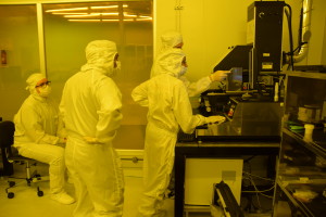
Clean room 1 (4)

The Centre offers admission to the Ph. D. degree program of the Institute under two streams, as described below. These programs involve rigorous course work followed by thesis research in various fields, including nanomaterials and nanostructures, electronics, nanofluidics, nanophotonics, nanobiotechnology, plasmonics, sensor systems, computational modeling etc.

Duration: Variable (typically four to six years) although there have been exceptional instances where PhD thesis have been successfully defended under 2.5 years

To apply click here

Direct Admission (denoted as NE stream)

The NE stream provides direct admission to the Ph.D. program of the Centre run by its faculty. Research Areas: Nanomaterials and Nanostructures, Nanoelectronic Devices, Nanoscale motion, Nano-Biophotonics, Nanophotonics, Plasmonics, Sensor Systems and Computational Nanoengineering.
To apply click here

DSC04724

Interdisciplinary Program (denoted as NA stream)

The second stream is an interdisciplinary program conducted by the Centre in conjunction with several other departments across the Institute. A student admitted under this program has two advisors from two different departments. The admission into this program is offered against a specified research project proposed by the two advisors. A list of all available projects is made available to admission seekers before the interview.

Research Areas: Broadly, all areas of nano science and engineering.

Eligibility for the PhD programs:

  • M.E./M.Tech. or equivalent in any discipline.
  • B.E. / B.Tech. or equivalent in any Engineering discipline with a valid score in a recommended GATE paper (See list of papers for M.Tech)
  • M.Sc. or equivalent in any Science discipline with a valid score in a recommended GATE paper (See list of papers for M.Tech)
  • Qualification in one of the following national exams: INSPIRE, Joint CSIR UGC NET for JRF, DBT JRF, UGC NET for JRF and JEST.

To apply click here

M Tech program: Admission to the M Tech program is offered only for the July session.

Ph. D program: Admissions to the PhD program is typically done for the July session. However, a limited number of topic/field specific admissions may be made for the January session as well. 

The admission process starts with filing the online applications at the IISc admissions website. Candidates are shortlisted for interview based on either the scores in one of the national exams or qualification. The detailed eligibility criteria can be found here. The background of students admitted to CeNSE in the past have been mostly from ECE, Physics, Mechanical, Materials disciplines, although there are students pursuing PhD/ MTech at CeNSe whose undergraduate degrees are in areas as diverse as biotechnology or biomedical instrumentation. Shortlisted candidates have to appear for an interview at CeNSE for selection. The interview typically consists of two to three sections, namely math and analytical questions such as plotting functions, basic calculus, differential equations etc, questions related to courses taken during their UG and PG degrees, and questions probing their research aptitude. Admission is based primarily on the performance in the interview and the results are generally announced 2-3 weeks after the interview.

Post Admission M Tech

lab 2M Tech students typically spend most of their first year in taking courses. The course structure consists of a combination of core courses offered at CeNSE, and electives which the student may take from any department at IISc. Towards the end of the first semester, the students need to choose an M Tech thesis project which is an indispensible part of the successful completion of the M Tech program. Work related to the thesis starts during the 2nd semester and should result in a well documented report culminating in the award of the M Tech degree.
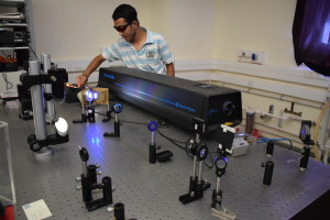
Post Admission Ph. D

The most important activity after joining the Ph. D program is the selection of your research advisor. At CeNSE we give absolute freedom to choose a research advisor based on the mutual interest of the student and the faculty member. In order to make a well thought out choice of research advisor, you are encouraged to talk to the faculty members whose work interest you and spend some time in their labs and attend the group meetings to get a good idea of what research in the group involves.

Students typically take between 4-8 courses depending on the prior preparation to gain a solid background in their topic of research. They should maintain a minimum CGPA of 7 throughout the course program. A major step towards the completion of a successful PhD is to pass the comprehensive exam which is held before completing two years in the PhD program. The comprehensive exam is evaluated by a committee of examiners from inside and outside the department. The committee evaluates if sufficient progress has been made towards the research goal. The exam also tests your grasp of the material discussed in your course work. After successfully passing the comprehensive exams, students focus on the research problem intensively leading to the successful defense of the PhD thesis typically within 5 years of joining the program.

Prime Minister’s Research Fellowship (PMRF) Scheme 

For details check https://pmrf.in


January - April
NE 200 January - April Technical Writing and Presentation

This course is designed to help students learn to write their manuscripts, technical reports, and dissertations in a competent manner. The do's and don'ts of the English language will be dealt with as a part of the course. Assignments will include writing on topics to a student's research interest, so that the course may benefit each student directly.

Instructor: S.A. Shivashankar

NE 201 January - April Micro and Nano Characterization Methods

This course provides training in the use of various device and material characterization techniques. Optical characterization: optical microscopy, thin film measurement, ellipsometry and Raman spectroscopy; Electrical characterization: Noise in electrical measurements, Resistivity with 2- probe, 4-probe and van der Pauw technique, Hall mobility, DC I-V and High frequency C-V characterization; Mechanical characterization: Laser Doppler vibrometry, Scanning acoustic microscopy, Optical profilometry, and Micro UTM; Material characterization: Scanning electron microscopy, Atomic force microscopy, XRD, and Focused ion beam machining.

Instructors: Akshay Naik and Manoj Varma

NE 202 January - April Micro and Nano Fabrication

This course is designed to give training in device processing at the cleanroom facility. Four specific modules will be covered to realize four different devices i) p-n junction diode, ii) MOS capacitor iii) MEMS Cantilever iv) Microfluidic channel.

Instructors : Shankar Kumar Selvaraja and Sushobhan Avasthi

NE 211 January - April Micro/Nano Mechanics

This is a foundation level course in mechanics which will prepare students to pursue advanced studies related to mechanical phenomena at the micro and nano scales. Basics of continuum theory, continuum hypothesis, elasticity, thermoelasticity, fluid mechanics, heat conduction, electromagnetism, coupled thermal-elastic and electrostatic-elastic systems, MEMS and NEMS structures -- beams, plates, and membranes, scaling of mechanical properties and continuum limits, numerical methods for mechanical modelling, mechanics beyond continuum theory.

Instructors: Rudra Pratap, Akshay Naik and Prosenjit Sen

NE 221 January - April Advanced MEMS Packaging

This course intends to prepare students to pursue advanced topics in more specialized areas of MEMS and Electronic packaging for various real-time applications such as Aero space, Bio-medical, Automotive, commercial, RF and micro fluidics etc. MEMS – An Overview, Miniaturisation, MEMS and Microelectronics -3 levels of Packaging. Critical Issues viz., Interface, Testing & evaluation. Packaging Technologies like Wafer dicing, Bonding and Sealing. Design aspects and Process Flow, Materials for Packaging, Top down System Approach. Different types of Sealing Technologies like brazing, Electron Beam welding and Laser welding. Vacuum Packaging with Moisture Control. 3D Packaging examples. Bio Chips / Lab-on-a chip and micro fluidics, Various RF Packaging, Optical Packaging, Packaging for Aerospace applications. Advanced and Special Packaging techniques – Monolithic, Hybrid etc., Transduction and Special packaging requirements for Absolute, Gauge and differential Pressure measurements, Temperature measurements, Accelerometer and Gyro packaging techniques, Environmental Protection and safety aspects in MEMS Packaging. Reliability Analysis and FMECA. Media Compatibility Case Studies, Challenges/Opportunities/Research frontier.

Instructors:  Prosenjit Sen and M.M. Nayak

NE 310 January - April Photonics technology: Materials and Devices

Optics fundamentals; ray optics, electromagnetic optics and guided wave optics, Light-matter interaction, optical materials; phases, bands and bonds, waveguides, wavelength selective filters, electrons and photons in semiconductors, photons in dielectric, Light-emitting diodes, optical amplifiers and Lasers, non-linear optics, Modulators, Film growth and deposition, defects and strain, III-V semiconductor device technology and processing, silicon photonics technology, photonic integrated circuit in telecommunication and sensors.

Instructor:  Shankar Kumar Selvaraja

NE 313 January - April Lasers: Principles and Systems

This is an intermediate level optics course which builds on the background provided in “Introduction to photonics” offered in our department. Owing to the extensive use of lasers in various fields, we believe a good understanding of these principles is essential for students in all science and engineering disciplines.

Instructor: V R Supradeepa

NE 332 January - April Physics and Mathematics of Molecular Sensing

This course presents a systematic view of the process of sensing molecules with emphasis on bio-sensing using solid state sensors. Molecules that need to be sensed, relevant molecular biology, current technologies for molecular sensing, modeling adsorption-desorption processes, transport of target molecules, noise in molecular recognition, proof-reading schemes, multi-channel sensing, comparison between in-vivo sensing circuits and solid state biosensors.

Instructor: Manoj Varma

August - December
NE 201 August - December Micro and Nano Characterization Methods

This course provides training in the use of various device and material characterization techniques. Optical characterization: optical microscopy, thin film measurement, ellipsometry and Raman spectroscopy; Electrical characterization: Noise in electrical measurements, Resistivity with 2- probe, 4-probe and van der Pauw technique, Hall mobility, DC I-V and High frequency C-V characterization; Mechanical characterization: Laser Doppler vibrometry, Scanning acoustic microscopy, Optical profilometry, and Micro UTM; Material characterization: Scanning electron microscopy, Atomic force microscopy, XRD, and Focused ion beam machining.

Instructors:  Akshay Naik and Manoj Varma.

NE 202 August - December Micro and Nano Fabrication

This course is designed to give training in device processing at the cleanroom facility. Four specific modules will be covered to realize four different devices :

  1. p-n junction diode
  2.  MOS capacitor
  3. MEMS Cantilever
  4. Microfluidic channel.

Instructors: Shankar Kumar Selvaraja and Sushobhan Avasthi

NE 203 August - December Advanced micro- and nanofabrication technology and process

Introduction and overview of micro and nano fabrication technology. Safety and contamination issues in a cleanroom. Overview of cleanroom hazards. Basic process flow structuring. Wafer type selection and cleaning methods. Additive fabrication processes. Material deposition methods. Overview of physical vapour deposition methods (thermal, e-beam, molecular beam evaporation) and chemical vapour deposition methods (PE-CVD, MOCVD, CBE, ALD). Pulsed laser deposition (PLD), pulsed electron deposition (PED). Doping: diffusion and ion implant techniques. Optical lithography fundamentals, contact lithography, stepper/canner lithography, holographic lithography, direct-laser writing. Lithography enhancement methods and lithography modelling. Non-optical lithography; E-beam lithography, ion beam patterning, bottom-up patterning techniques. Etching process: dry and wet. Wet etch fundamentals, isotropic, directional and anisotropic processes. Dry etching process fundamentals, plasma assisted etch process, Deep Reactive Ion Etching (DRIE), Through Silicon Vias (TSV). Isotropic release etch. Chemical-mechanical polishing (CMP), lapping and polishing. Packaging and assembly, protective encapsulating materials and their deposition. Wafer dicing, scribing and cleaving. Mechanical scribing and laser scribing, Wafer bonding, die-bonding. Wire bonding, die-bonding. Chip-mounting techniques.

Instructors: Shankar Kumar Selvaraja and Sushobhan Avasthi

NE 205 August - December Semiconductor Devices and Integrated Circuit Technology

This is a foundation level course in the area of electronic device technology. Band structure and carrier statistics, Intrinsic and extrinsic semiconductor, Carrier transport, p-n junction, Metal-semiconductor junction, Bipolar Junction Transistor, Heterojunction, MOS capacitor, Capacitance-Voltage characteristics, MOSFET, JEFET, Current-Voltage characteristics, Light Emitting Diode, Photodiode, Photovoltaics, Charge Coupled Device Integrated circuit processing, Oxidation, Ion implantation, Annealing, Diffusion, Wet etching and dry plasma etching, Physical vapour deposition, Chemical vapour deposition, Atomic layer deposition, Photolithography, Electron beam lithography, Chemical mechanical polishing, Electroplating, CMOS process integration, Moore’s law, CMOS technology scaling, Short channel effects, Introduction to Technology CAD, Device and Process simulation and modelling.

Instructor: Digbijoy N. Nath

NE 213 August - December Introduction to Photonics

This is a foundation level optics course which intends to prepare students to pursue advanced topics in more specialized areas of optics such as biophotonics, nanophotonics, non-linear optics etc. Classical and quantum descriptions of light, diffraction, interference, polarization. Fourier optics, holography, imaging, anisotropic materials, optical modulation, waveguides and fiber optics, coherence and lasers, plasmonics.

Instructors: Shankar Kumar Selvaraja and Ambarish Ghosh

NE 215 August - December Applied Solid State Physics

This course is intended to build a basic understanding of solid state science, on which much of modern device technology is built, and therefore includes elementary quantum mechanics. Review of Quantum Mechanics and solid state physics, Solution of Schrodinger equation for band structure, crystal potentials leading to crystal structure, reciprocal lattice, structure-property correlation, Crystal structures and defects, X-ray diffraction, lattice dynamics, Quantum mechanics and statistical mechanics, thermal properties, electrons in metals, semiconductors and insulators, magnetic properties, dielectric properties, confinement effects.

Instructors: Akshay Naik and S A Shiva Shankar

NE 222 August - December MEMS: Modeling, Design, and Implementation

This course discusses all aspects of MEMS technology – from modeling, design, fabrication, process integration, and final implementation. Modeling and design will cover blockset models of MEMS transducers, generally implemented in SIMULINK or MATLAB. Detailed multiphysics modeling may require COMSOL simulations. The course also covers MEMS specific micromachining concepts such as bulk micromachining, surface micromachining and related technologies, micromachining for high aspect ratio microstructures, glass and polymer micromachining, and wafer bonding technologies. Specific case studies covered include Pressure Sensors, Microphone, Accelerometers, Comb-drives for electrostatic actuation and sensing, and RF MEMS. Integration of micromachined mechanical devices with microelectronics circuits for complete implementation is also discussed.

Instructors: K.N. Bhat and Saurabh A. Chandorkar

NE 223 August - December Analog Circuits and Embedded System for Sensors

The Internet of Things (IoT) revolution is driven by confluence of high performance sensors, powerful computation power of microcontrollers and wireless technology. The performance of sensors is not only governed by inherent characteristics of sensor such as sensitivity, linearity and response time but also the front end interfacing analog circuit and backend processing in digital domain. The goal of this course is to explore the electronics that needs to be incorporated to create sensor systems and to learn the trade-offs in design of circuits to maximize performance subject to real life design constraints.

The course has both a theory (2 credits) and a hands-on lab (1 credit) element to it. The course starts out with introduction to basic circuit elements and smaller circuit building blocks with emphasis on reading and understand the datasheets for components to make the appropriate choice to pick for the circuit at hand.  Digital IOs and some basics of digital logic will be explored thereafter leading eventually to programming with Arduino microcontroller. In the end, the course takes a closer look at building systems.

The lab portion of the course will serve to explore trade-offs in circuit design as well as give a practical feel for dealing with noise in circuits and building systems. Circuit simulation will also be emphasized in the lab course in conjunction with back of the envelop calculations to make sense of the simulations. There will be also be a final project wherein the students get an opportunity to build a sensor system in its entirety and learn planned system design, tracking down sources of noise and learning to define interfaces cleanly for smooth integration in the end.

The course content is as follows:

Basic Circuit Analysis and Passive Components; Introduction to semiconductor devices and circuits involving Diodes, BJT, MOSFET and JFET; Opamp circuits: Transimpedance amplifier, Instrumentation amplifier, Comparator, Precision DMM application; Tradeoffs between power, noise, settling time and cost; Survey of sensors and their datasheets; Active Filters and RF Oscillators; Introduction to digital logic, State Machines, Digital IO; Microcontroller programming; Communication protocols for sensor interfacing; System building

Instructors: Saurabh A. Chandorkar and Krishna Prasad


NE 231 August - December Microfluidics

This is a foundation course discussing various phenomena related to fluids and fluid-interfaces at micro-nano scale. This is a pre-requisite for advanced courses and research work related to micro-nano fluidics. Transport in fluids, equations of change, flow at micro-scale, hydraulic circuit analysis, passive scalar transport, potential fluid flow, stokes flow Electrostatics and electrodynamics, electroosmosis, electrical double layer (EDL), zeta potential, species and charge transport, particle electrophoresis, AC electrokinetics Surface tension, hysteresis and elasticity of triple line, wetting and long range forces, hydrodynamics of interfaces, surfactants, special interfaces Suspensions, rheology, nanofluidics, thick-EDL systems, DNA transport and analysis.

Instructor: Prosenjit Sen

NE 241 August - December Material Synthesis: Quantum Dots To Bulk Crystals

All device fabrication is preceded by material synthesis which in turn determines material microstructure, properties and device performance. The aim of this course is to introduce the student to the principles that help control growth. Crystallography; Surfaces and Interfaces; Thermodynamics, Kinetics, and Mechanisms of Nucleation and Growth of Crystals ; Applications to growth from solutions, melts and vapors (Chemical vapor deposition an Physical vapor deposition methods); Stress effects in film growth.

Instructor: Srinivasan Raghavan

NE 250 August - December Entrepreneurship, Ethics and Societal Impact

This course is intended to give an exposure to issues involved in translating the technologies from lab to the field. Various steps and issues involved in productization and business development will be clarified, drawing from experiences of successful entrepreneurs in high technology areas. The intricate relationship between technology, society and ethics will also be addressed with illustrations from people involved in working with the grass root levels of the society.

Instructor: Navakanta Bhat

NE 312 August - December Nonlinear and Ultrafast Photonics

This is an intermediate level optics course which builds on the background provided in “Introduction to photonics” offered in our department. Owing to the extensive use of nonlinear optical phenomena and Ultrafast lasers in various fields, we believe a good understanding of these principles is essential for students in all science and engineering disciplines, in particular students involved in the area of Photonics, RF and Microwave systems, Optical Instrumentation and Lightwave (Fiber-optic) Communications. In addition, this course intends to prepare students to pursue advanced topics in more specialized areas of optics such as Biomedical Imaging, Quantum optics, Intense field phenomena etc.

Instructor: V. R. Supradeepa


Course timings for the semester (Jan - April 2024) is as follows:

Sl. No Course code Topic Instructors Time Day First Class Classroom
1. NE 201 B 0:2 Lab for structural and functional characterization Prof.Akshay Naik 2 to 5 pm Monday to Friday 04th Jan

Lab

Teams link

2. NE 202 0:2 Micro and Nano Characterization Prof.Sushobhan Avasthi 2 to 4 pm Monday Wednesday Thursday Friday 03rd Jan

Lab

Teams link

3 NE 221 2:1 Advanced MEMS Packaging Prof. Prosenjit Sen 09:00 to 10:00 am  Monday Wednesday Friday 03rd Jan

FF-11, CeNSE

Teams Link

4 NE 223 2:1 Analog Circuits and Embedded System for Sensors Prof. Saurabh Arun Chadorkar 04:00 to 05:00 pm Monday Wednesday Friday 08th Jan

TF-10, CeNSE

Teams Link

5.

NE 235 3:0

Microsystem Design and Technology

Prof. Gayathri Pillai 

10.00 to 11.30 am

Tuesday Thursday

04th Jan

FF-11, CeNSE

Teams Link

6. NE 241 3:0 Material Synthesis : Quantum Dots to Bulk Crystals Prof. Pavan Nukala 2:00 to 3:30 pm Tuesday Thursday 02nd Jan

FF-11, CeNSE

Teams Link

7. NE 299 0:27 Disseratation Project Prof. Supradeepa V R      

Teams  Link

8.

NE 310 3:0 Photonics technology: Materials and Devices Prof.Shankar Kumar Selvaraja

11:30 am to 01:00 pm

Tuesday Thursday

02nd Jan

FF-11, CeNSE

Teams Link

9.

NE 311 1:1 Integrated photonics Lab Prof.Shankar Kumar Selvaraja 12.00pm to 1:00 pm


Monday Wednesday Friday 03rd Jan

FF-11, CeNSE

Teams Link

10.

NE 312 3:0

Nonlinear and Ultrafast Photonics 

Prof. Supradeepa V R ,  Prof Varun Raghunathan

2.00 to 3.30 pm 

Monday Wednesday 

03rd Jan

ECE 1.08, FF11 (From March)

Teams Link

11. NE 314 3:0 Semiconductor Opto-electronics and Photovoltaics Prof. Aditya Sadhanala 10.00 am to 11:30 am Tuesday Thursday 04th Jan

TF-10, CeNSE

Teams Link

12.

NE 317 3:0

From natural to artificial intelligence

Prof. Sreetosh Goswami

3:30 to 5:00 pm 

Tuesday Thursday

04th Jan

FF-11, CeNSE

Teams Link

13. NE 320 3:0

Quantum Optics 

Prof. Supradeepa V R, Prof. Baladitya Suri

3:30 pm to 5:00 pm

Monday Wednesday

08th Jan

FF-11, CeNSE

Teams Link

14. NE 332 3:0 Physics and Mathematics of Molecular Sensing Prof. Manoj Varma 10:00 to 11.30 am Monday Wednesday 08th Jan

FF-11, CeNSE

Teams Link

Course timings for the semester (Aug - Dec 2023) is as follows :

Sl. No Course code Topic Instructors Time Day Classroom First Class
1. NE 200    

Technical Writing and Presentation

Prof. Sreetosh Goswami/ Prof. Shivashankar

03.00 pm to 05.00 pm

Wednesday Seminar Hall

09th August

Teams Link

2. NE 201A     

Theory of structural and functional characterization

Prof. Akshay K Naik / Prof. Gayathri Pillai

12.00 pm to 01.00 pm

Monday Wednesday Friday

FF-11 MMCR

02nd August

Teams Link

3. NE 202 Micro and Nano Fabrication Prof. Sushobhan Avasthi 02:00 pm to 04:30 pm Monday Wednesday Thursday Seminar Hall

2nd August

Teams Link

4. NE 203    

Advanced micro and nano fabrication technology and process

Prof. Sushobhan Avasthi

11.30 am to 01.00 pm

Tuesday Thursday FF11 MMCR

01st August

Teams Link

5. NE 206 

Semiconductor Device Physics: Basics Devices

Prof. Sushobhan Avasthi

10.00 am to 11.00 am

Monday Wednesday Friday TF10

02nd August

Teams Link

6. NE 213   

Introduction to Photonics

Prof. Ambarish Ghosh/ Prof. Shankar  Kumar Selvaraja

10.00 am to 11.30 am

Tuesday Thursday FF-11 MMCR

03rd August

Teams Link

7. NE 215    

Applied Solid State Physics 

Prof. Akshay K Naik 

11:00 am to 12.00 pm

Monday Wednesday Friday FF-11 MMCR

02nd August

Teams Link

8. NE 222  

MEMS: Modeling, Design, and Implementation  

Prof. Saurabh Arun Chandorkar/ Prof. Gayathri Pillai

03.30 pm to 5.00 pm

Monday Friday FF-11 MMCR

04th August

Teams Link

9. NE 231 

Microfluidics 

Prof. Prosenjit Sen 

02.00 pm to 03.30 pm

Monday Wednesday Friday FF-11 MMCR

02nd August

Teams Link

10.

NE 240

Materials design principles for electronic, electromechanical and optical functions  

Prof. Pavan Nukala 

02.00 pm to 03.30 pm

Tuesday Thursday

FF-11 MMCR

03rd August

Teams Link

11. NE 250 

Entrepreneurship, Ethics and Societal Impact 

Prof. Navakanta Bhat 

05.00 pm to 06.00 pm

Monday FF-11 MMCR

07th August

Teams Link

12. NE 281   

Statistical and probabilistic data analysis techniques 

Prof. Manoj Varma

03.30 pm to 05.00 pm

Tuesday Thursday FF-11 MMCR

03rd August

Teams Link

13. NE 316   

Advanced Electron Microscopy in Materials Characterization 

Prof.Pavan Nukala 10:00 am to 11:30 am Tuesday Thursday TF10

03rd August

Teams Link

14. NE 352    

Quantum transport in low dimensional materials 

Prof. Chandan Kumar 03:30 pm to 05:00 pm Tuesday Thursday TF10

1st August

Teams Link

Starting from 2013, the centre conducts a training program every summer, for promising Undergraduate and Masters students from India and abroad, selected through a rigorous and competitive process. The training is primarily based on the facilities available at CeNSE, and covers a variety of research topics under the broad umbrella of nano science and engineering. The training program will be of 8 -10 weeks duration. The scholarship paid to the eligible candidates would be Rs 5000/month.

How to apply:

Every January we put up online forms in Homepage for applying to the summer program. Post selection, the list of selected candidates is displayed here.  Last date to submit the application is 28th February 2024.

Apply Here


Selected candidate list - 2023

Name of the Student College
Abhishek Raj Indian Institute of Technology Madras, Chennai
Aditya Katiyar Indian Institute of Technology (BHU) Varanasi
Adway Paul Jadavpur University
Ajit Gupta BMS College of Engineering
Alankit Dey IIT Madras
Amitesh Gupta Indian Institute of Science, Education and Research, Mohali
Ananya Kalita National Institute of Technology Silchar
Anurit Dey Indian Institute of Science Education and Research (IISER), Kolkata
Anurag Hegde Birla Institute of Technology and Science (BITS), Pilani
Arkapravo Ghosh Indian Institute of Technology Kharagpur
Bipin Kumar Indian Institute of Technology Delhi
B. Harsha Vardhan National Institute of Technology Calicut
Diptanu Debnath National Institute of Technology Agartala
Dr. Pooja P Jain Indian Institute of Technology, Kharagpur
Farhaan Iqbal IIT BHU
GAUREESHA KAJAMPADY IIT HYDERABAD
Gargi Thakur Indian Institute of Science Education and Research (IISER), Bhopal
Jeet Das Jadavpur University
Kandarp Solanki Indian Institute of Technology Bombay
MEDAGAM SRI MADHURIMA National Institute of Technology Karnataka, Surathkal
MEDICHARLA V K RAJEEV SRIKAR Indian Institute of Technology Kharagpur
Mohammed Areeb Hussain IIT Hyderabad
Navdha IIT Bombay
Palak Gupta National Institute of Technology Meghalaya
Prajjwal Sanskar IISER, Bhopal
Prakyath T P BMS College of Engineering
Premkumar Iyer National Institute of Technology Calicut
Rajarshi Mukherjee Jadavpur University
Rahul Bouri Birla Institute of Technology and Sciences, Pilani
Rohan Thomas Mathew National Institute of Science Education and Research
Rithwik Raina Indian Institute of Science Education and Research, Kolkata
Shivani Chhipa IIT kharaghpur
Swapnil Dey National Institute of Technology Agartala
Sourin Das Indian Institute of Science Education and Research, Bhopal(IISER Bhopal)
Trideeb Bhattacharya Birla Institute of Technology and Science Pilani, Pilani Campus
V.Prithiv ICT Mumbai IOC Bhubaneshwar

  1. Do the students have a flexibility in joining date (exams etc.,)?
    The intern has to join the program before 31st May, and should spend at least 8 weeks.
  2. Which Faculty details to be provided in the Application? 
      Faculty is your faculty under whom you are studying at present, not IISc faculty with whom you will work during your internship.
  3. Eligibility criteria – students studying in various stages of UG/PG?
    Anybody actively enrolled in a degree program (UG/PG) will be eligible. If the student is graduating before the start of summer (May), he/she will not be eligible.
  4. Currently student, by start of the program one would get graduated, is this a constraint?
    See before
  5. To whom should we write for any further queries regarding the program?
    Send your queries to summerinterncense@gmail.com
  6. Any accommodation will be provided to participants of the summer program?
    No accommodations will be provided to the participants.

A few more points to be noted:

These internship positions are industry sponsored and you will receive a sum of Rs 5000/- (Rupees five thousand) per month of your stay.

  1. You are expected to stay at the Centre for a minimum of 8 weeks. Requests for shorter internship periods will not be considered.
  2. You will be responsible for arranging your accommodation.
  3. An oral presentation would have to be made by you at the end of your stay.

Name of the Student College
A Vignesh Indian Institute of Science Education and Research, Mohali
Abhinav Kumar Gupta National Institute of Technology, Silchar
Abhishek S Cochin University of Science and Technology
Amit Rohan Rajapurohita Purdue University
Anomitra Banerjee Jadavpur University
Chayan Debbarma National Institute of Technology Agartala
DHANASURYA S CSIR-Central Electrochemical Research Institute.
Drik Sarkar Indian Institute of Technology Kharagpur
Devashish Girish Bhave Indian Institute of Technology, Bombay
G L Venkat Laxmi The National Institute of Engineering
G Vinaya Sri National Institute of Technology Andhra Pradesh
JAHNAVI M S IISER THIRUVANANTHAPURAM
KOUSHIK MEDHI IISER BHOPAL
LAKSHMI U COCHIN UNIVERSITY OF SCIENCE AND TECHNOLOGY
Likhitha K MS ramaiah University of applied sciences
Milisha Mahapatra National Institute of Technology Sikkim
Pratik Pal Indian Institute of Science Education and Research(IISER), Bhopal
Rajesh Kashyap Indian Institute of Technology Gandhinagar
Riddhi Chakraborty Jadavpur University
Sanna Showkat National Institute of Technology, Srinagar.
Sarit Roy Chaudhury Jadavpur University
Shaik Dilshad Begum National Institute of Technology Surathkal, Karnataka
Sneha Mary Biju National Institute of Technology, Calicut
Subhashis Ghosh National Institute of Science Education and Research(NISER)
Sukrit Dass T M National Institute of Technology Karnataka, Surathkal
Sukanya Panja Indian Association for the Cultivation of Science
Tanmoy Pati National Institute of science education and research,Bhubaneswar
Ujjwal Chaudahry NIT Hamirpur
Vaibhav Nagrale NIT Trichy
Yash Patel National Institute of Technology Karnataka, Surathkal

Name of the student College
Panda Sarthak Shantanoo Indian Institute of Technology (Indian School of Mines) Dhanbad
Jatin Arora Birla Institute of Technology and Science (BITS) - Pilani
Rupayan Sarkar Indian Institute of Technology, Kharagpur
Agnivarna Trivedi National Institute of Technology,Durgapur
Varun Kumar M National Institute of Technology Karnataka
SHYAM KUMAR L NATIONAL INSTITUTE OF TECHNOLOGY , TRICHY
Ujjwal Chitnis National Institute of Technology Raipur
Saksham Mahajan IISER MOHALI
Vidhukiran Venkataraman BITS Pilani Hyderabad Campus
Manan Atul Suraiya National Institute of Technology, Tiruchirappalli
Aditya Ashutosh National Institute of Technology, Agartala, Tripura
Rishav Mansuri Indian Institute of Technology Roorkee
Atif Jan BITS-Pilani
ANKUR SINGH Indian Institute of Science, Bangalore
Ayman Urfa University of Waterloo
Nabasindhu Das IIT Roorkee
P Sree Harsha IIT Madras
Abdul Qadir M S Ramaiah Institute of Technology
Ipsita Panda National Institute of Technology, Tiruchirapalli
K.Nomalatha National Institute of Technology, Warangal
Swathilakshmi NITK, Surathkal
Aniruddh Holemadlu Nitte Meenakshi Institute of Technology
Pavithra Venkataraman Ramaiah Institute of Technology
K.S.Akkash scsvmv deemed to be university
Shashank Tripathi SRM Institute of Science and Technology, Kattankulathur, Chennai, Tamil Nadu
Harshita Thakur National Institute of Technology Raipur

Name of the student College
Renuka M IISER TVM
Arpit Jain NIT TRICHY
Aditya Shah NIT-K Surathkal
Shwetha S Kumar NIT Trichy
Athulya Babu NIT TRICHY
Harshitha.S IIT MADRAS
Nidhi Malhotra IIT BHU Varanasi
Sudeshna Sen NIT Durgapur
Sneha Banerjee NIT Durgapur
Shreyans Tiwari IIT (BHU) Varanasi
Mohit Jain NIT Raipur
Shruti Pandey NIT RAIPUR
Nikhil Navaratna BITS Pilani Hyderabad Campus
Sagar IIT Delhi
Sparsh Agarwal Iowa State University 
Aniket Ghangas NIT Kurukshetra
Pema Wanchuk Lama NMIT
Vaibhav Verma CBS Mumbai
Nikhil Utsav NIT Arunachal Pradesh
Fasil C IISER BHOPAL
Midhush Manohar T.K. PES University
Vaibhav Sharma BITS-Pilani hyderabad Campus
Velury Suguna Varshini Ramaiah Institute of Technology
   

Name of the student College
Abhishek Upadhyay National Institute Of Technology Nagaland
Aditya Tripathi IIT Delhi
Anish Pradhan National Institute Of Technology Durgapur
Anwesha Saha University of Massachusetts Amherst
Deeksha Pai S National Institute Of Technology, Karnataka, Surathkal
Divyam Tayal Jamia Millia Islamia University, New Delhi
Elizabath Peter National Institute Of Technology, Calicut, Kerala
Farsana N A

National Institute Of Technology Calicut, Kerala

Haley Wohlever University of Rochester, New York, USA
Monalisa Mallick Defence Institute of Advanced Technology,Pune, Maharashtra
Purbesh Mitra Jadavpur University, Kolkata
Rebecca Ananya Mathias Ramaiah Institute of Technology
Ritwik Vatsyayan IIT Guwahati
S Suparna Indian Institute of Technology  Madras, Chennai
Sai Venkata Gayathri A National Institute Of Technology Tiruchirappalli
Sanjana S R V College Of Engineering
Tanvi Verma Indian Institute of Technology  Roorkee
   

Name of the student College
Arkadev Roy IIT Kharagpur
Praneeth Srivanth R IIT Madras
Sanmathi Kamath National Institute Of Technology, Surathkal
Rajarshi Khan IIT Kharagpur
Krishna Chaitanya IIT Madras
Archana Balan VIT University, Vellore,Tamil Nadu, India
Arun Mahesh B.M.S College Of Engineering. Karnataka
Anagha Kamath SVNIT, Surat
Varun Raj K    CUSAT
Aratrika Ghose NIT, Rourkela
Kiran Singh IIT Patna, Bihta,Bihar
Arthi Eswaran National Institute Of Technology,Tiruchirappalli
Jayanthi Akhil    National Institute Of Technology, Durgapur
Ankit Raj    Indian Institute Of Technology, Kanpur
Siddharth Lal    IIT Kanpur
Aamir Faisal Ansari Visvesvaraya National Institute Of Technology, Nagpur
Aditya Panda Jadavpur University
Neeraj Kaushal National Institute Of Technology, Hamirpur
Anukta Datta National Institute Of Technology, Rourkela
Akash Singh PDPM IIITDM
Ishan Sharma Birla Institute Of Technology And Science, Pilani
Shifa Nizami National Institute Of Technology, Uttarakhand
Mukul Sharma Indian Institute Of Technology- Banaras Hindu University(Varanasi)
Mahesh Yogi IIT Guwahati
Om Kesharwani National Institute Of Technology, Arunachal Pradesh

Name of the student College
Abhay Nayak LIT Madras
Abhijith R B.M.S College of Engineering, Bangalore
Adarsh Senapati IIT Guwahati
Akash Sinha National Institute of Technology, Durgapur, India
Anmol Jain National Institute of Technology, Hamirpur
Avratanu Ghosh Jadavpur University
Ayan Biswas IIT Kharagpur
Chittaranj an Baliarsingh National Institute of Technology, Rourkela
Gaurav Garg IIT Roorkee
Geethika Muralidharan International School of Photonics, Cochin University
Guillaume Blot Ecole Normale Superieure of Lyon
Harish K National Institute of Technology, Trichy
Mahathi Anand SRM University
Moullick Sonar College of Engineering, Pune
Omkar Mehta Institute of Chemical Technology
Rohm Mahapatra National Institute of Technology Sikki
Shashank Tripathi Birla Institute of Technology and Science, Pilani
Shivam Chopra PEC University of Technology
Shriddha Chaitanya National Institute of Technology, Surathkal
Sowmya L National Institute Of Technology Calicut
Subhajit Karmakar National Institute Of Technology, Delhi
Swayam Tibrewal VIT University
Vishwanathan Giridar IIT Madras
Washim Alam IIT Kharagpur

Name of the student College
Mallika Bariya Cornell University, New York
Madhav Gupta University of Southern California
Kunal Soni IISc Bangalore
Ani Jose Cochin University of Science and Technology
Kuldeep Reddy SRM University
Subhajit Mohanty IIT KANPUR
Pratyush Srivastava Maulana Azad National Institute of Technology, Bhopal
Saket Bhargava BITS – Pilani
Ameet Rajput Maulana Azad National Institute Of Technology
Dandamudi Chola Bhargava IIT, Guwahati
Arun Krishnadas IITM
Chhavi Choudhary IIT ROORKEE
Jishnu Dey IIT Kharagpur
Aranya Goswarai IIT, Kharagpur
Robin Singh National Institute Of Technology Karnataka, Swath
Arghya Patra IIT, Kharagpur

Name of the student College
Mayank Singh Mudgal IIT, Madras
Aneesh.Dash IIT, Bhubaneswar
Preeti.Deshpande Amity Institute of Nanotechnology
Vijay.Ramakrishnan NITK, Surathkal
Deepanshu Mishra IIT, Kanpur
Ravindra Jha NIT, Bhopal
Saee.Vyawahare BITS, Pilani
Sooraj.KP IISER, Bhopal
Vellaluru.Neeharika BITS, Pilani
Moab. Rajan Philip NITK, Surathkal
Himanshu.Jaiswal IIT, Jodhpur
Puneet Jain IIT, Roorkee
Punnag Padhy IIT, Bhubaneswar
Prithivirajan.S R IIT, Bhubaneswar
Soumya.Yandrapalli NITK, Surathkal